Ceramic Packages with Leads: Types, Applications, and Design Guidelines
-
2026-04-03 Industry News


This book systematically explains everything from the structural principles of Leaded Ceramic Packages to representative package types (DIP and SIP packages), application fields, and key design points.
Introduction
Against the backdrop of the ongoing evolution of electronic packaging toward miniaturization and high performance, ceramic packages have gradually become a key choice for specific applications due to their material properties. Among these, leaded ceramic packages continue to enjoy stable market demand in terms of structural connection methods and application adaptability. Compared to purely surface-mount structures, these packages offer distinct advantages in assembly methods, stress relief, and ease of maintenance, making them suitable for electronic systems that require reliable connections.
What Are Leaded Ceramic Packages?
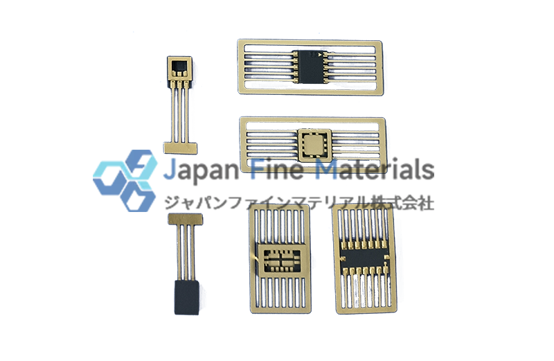
Leaded ceramic packages refer to a type of electronic packaging that uses ceramic material as the main body and achieves electrical connections through external metal leads. Within the structure of electronic devices, this type of package typically serves multiple functions, including chip protection, electrical connection, and structural support.
In terms of composition, their core consists of the following components:
• Ceramic substrate: Common materials include aluminum oxide (Al₂O₃) or aluminum nitride (AlN)
• Chip mounting area: Used to secure the semiconductor chip
• Wire bonding (gold wires): Establishes electrical connections between the chip and the leads
• External leads: Route internal signals to connect with external circuit systems
• Package structure: Used to isolate the internal device from the external environment
Compared to other packaging forms, the key distinction lies in the configuration of the external pins. These pins typically extend from the side or bottom of the package and can be used for through-hole mounting or partial surface-mount processes, providing a relatively intuitive connection path during PCB assembly.
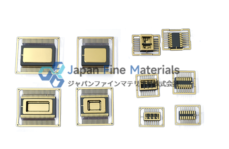
Types of Pin-Type Ceramic Packages
Depending on the pin structure and package layout, pin-type ceramic packages can be further classified into various types. Different structures have distinct characteristics in terms of pin distribution, assembly methods, and suitability for circuit complexity.
Ceramic Dual In-line Package (CDIP)
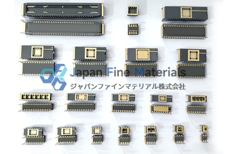
The CDIP package is a classic type of pin-type ceramic package. The pins are distributed on both sides of the package and are typically used for through-hole mounting. It has been widely and reliably used in early and some industrial electronic systems, facilitating structural connections and post-installation maintenance.
Structural Features:
• Dual-row through-hole pins, facilitating through-hole soldering and secure mounting
• Relatively wide pin spacing, which facilitates circuit layout and maintenance
• Mature packaging structure with stable manufacturing and assembly processes
• The ceramic substrate offers excellent electrical insulation and environmental adaptability
Applications:
CDIP is commonly used in applications requiring a certain level of installation stability and maintenance convenience, such as industrial control circuits and basic communication modules. In systems requiring manual insertion or component replacement, this packaging format is easier to integrate into the overall structural design.
Ceramic Flat Package (CFP)
CFP features a flat lead structure, with leads typically extending from the side of the package. Its overall structure is relatively compact, offering advantages in space utilization and height control, making it suitable for circuit designs with strict dimensional constraints.
Structural Features:
• Flat external lead design facilitates mounting and soldering
• Thin package profile helps reduce overall height
• Pins extend from the side, accommodating various PCB layout configurations
• Ceramic construction provides stability under varying temperature conditions
Applications:
CFP is particularly suitable for electronic modules with space constraints or height limitations, such as compact PCB designs or systems with high structural integration, helping to optimize the overall layout.
Ceramic Quad Flat Package (CQFP)
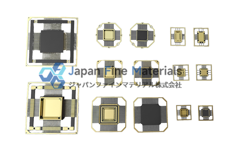
CQFP features pins on all four sides, making it suitable for integrated circuits with a high pin count. It offers greater adaptability for multi-signal connections and complex circuit layouts, and is one of the most common multi-pin ceramic packaging formats.
Structural Features:
• Pins are evenly distributed on all four sides, supporting more electrical connection points
• High pin density, suitable for complex circuit system integration
• Supports surface-mount technology (SMT), facilitating automated production
• Ceramic packaging offers excellent dimensional stability
Applications:
CQFP is commonly used in applications requiring multi-signal processing or involving a certain level of circuit complexity, such as communication equipment, multi-signal processing modules, and various control-type integrated circuits, helping to achieve designs with higher integration.
Ceramic Small Outline Package (CSOP)
CSOP is a pin-type package developed in response to the trend toward miniaturization. It features a narrow pin pitch and a more compact overall size, facilitating high-density circuit layouts within limited space.
Structural Features:
• Small external pin structure, suitable for compact designs
• Narrow pin pitch facilitates higher wiring density
• Supports automated placement, improving assembly efficiency
• Precise control of package dimensions to meet miniaturization requirements
Applications:
CSOP is particularly suitable for electronic products with specific requirements for size and integration, such as small devices or modular circuit systems, where it facilitates higher component density in limited spaces.
Leaded vs. Leadless Packages
During the package selection process, pin-type and pinless structures are often considered together.
|
VS |
Leaded Ceramic Package |
Leadless Ceramic Package |
|
Connection Method |
External Pins |
Bottom Pads/Bumps |
|
Assembly Method |
Through-hole / Partial Surface Mount |
SMT Mounting |
|
Stress performance |
Pins can act as a buffer |
Stress is concentrated in the solder joint area |
|
Compact design |
Relatively low |
More compact |
From a design perspective, neither structure is inherently superior; the choice depends more on the specific application environment and assembly conditions.
Key Considerations for Design and Selection
In actual projects, the selection of pin-type ceramic packages often depends not only on the structural form but also requires a comprehensive evaluation of multiple factors.
1. Material Selection
The type of ceramic material directly affects the package’s thermal performance, electrical insulation properties, and overall stability:
• Aluminum Oxide (Al₂O₃): Widely used, offering good electrical insulation and basic mechanical strength
• Aluminum Nitride (AlN): Offers superior thermal conductivity and is suitable for module designs with higher thermal management requirements
In practical applications, material selection typically requires a comprehensive evaluation that considers both power dissipation levels and thermal design.
2. Pin Design
Pins not only serve an electrical connection function but also affect assembly efficiency and structural reliability:
• Pin pitch affects PCB layout density
• The number of pins determines the scale of signals that can be supported
• Pin configuration (straight, bent, etc.) affects soldering methods and installation processes
A well-designed pin layout helps improve assembly consistency and reduces the difficulty of subsequent maintenance.
3. Package Structure
Different package structures exhibit varying levels of environmental adaptability:
• Whether an airtight package is used
• Type of package housing (all-ceramic or composite structure)
• Package dimensions and thickness constraints
In applications requiring protection against moisture and contamination, the selection of the packaging structure is particularly critical.
4. Thermal Management Pathways
Although ceramic materials possess some thermal conductivity, overall heat dissipation performance still depends on system-level design, such as:
• The thermal conduction path between the chip and the substrate
• Whether additional heat dissipation structures (such as heat sinks or metal bases) are required
• Coordination between PCB-level design and thermal management
In high-power-density applications, thermal co-design between the package and the system is particularly important.
5. Matching Dimensions and Integration Level
Package dimensions must be coordinated with the overall system layout while meeting functional requirements:
• High-pin-count packages are better suited for complex circuits
• Smaller-sized packages help improve integration
• Different package types have significantly different impacts on layout and routing
Conducting package selection early in the design phase helps reduce the cost of subsequent adjustments.
Conclusion
Multi-pin ceramic packages still hold a significant place in today’s electronic packaging landscape, as their structural design offers greater flexibility in connectivity and design for specific applications. In practical projects, conducting a comprehensive evaluation by combining different package types helps improve the overall suitability of the solution.
If you are evaluating ceramic packaging solutions suitable for your project’s requirements, or need structural optimization and selection support for specific applications, please contact JFM. We offer a variety of ceramic packaging solutions to help your project achieve the most suitable choices in terms of structural design and application compatibility.


