What are the advantages of CLCC packaging?
-
2026-04-03 Industry News


This overview highlights their key benefits—excellent heat dissipation, high thermal resistance, reliability, and suitability for compact, high-density designs—along with features and typical applications.
Introduction
In electronic packaging design, the packaging form not only affects how the chip is mounted but also has a direct impact on thermal management, electrical performance, and long-term operational stability. As application environments and performance requirements continue to become more specialized, the Ceramic Leadless Chip Carrier (CLCC) has gradually become a common choice in certain specific scenarios.
Compared to conventional packaging formats, CLCC packaging is not suitable for all applications but is specifically tailored in terms of material properties and structural design. Understanding its basic structure and advantages helps make more informed packaging decisions during the early design stages.
What is a Ceramic Leadless Chip Carrier (CLCC)?
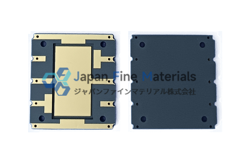
A Ceramic Leadless Chip Carrier (CLCC) is a leadless packaging format based on a ceramic substrate. Its core characteristics include:
• The use of a ceramic substrate as the carrier (typically aluminum oxide or aluminum nitride)
• No external leads; connection to the PCB is made via bottom metal pads
• Can be designed as either an open or covered package structure depending on requirements
Compared to traditional leaded packages, this structure offers greater compactness in terms of size control and connection methods, while also providing more flexibility for subsequent thermal design and electrical performance optimization.
Structure and Design of CLCC Packages
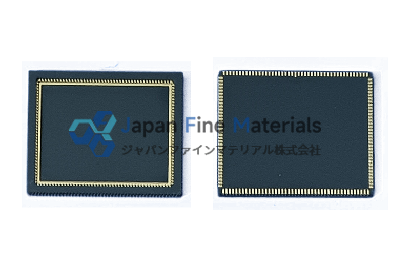
From an engineering perspective, the CLCC package is not simply a combination of "ceramic + pads"; its internal structure typically includes:
• Ceramic substrate: Provides mechanical support, electrical insulation, and a thermal conduction path
• Metallized interconnects: Used to establish signal and power connections
• Chip mounting area: Directly affects thermal resistance and reliability performance
• Package cover or sealing structure (optional): Used for environmental isolation
In actual design, different manufacturers may adjust metallization processes, stacking structures, or packaging formats to accommodate various application requirements.
Material Stability
The ceramic substrates (such as alumina and aluminum nitride) used in CLCC packages exhibit relatively stable physical and chemical properties, which is particularly critical under complex operating conditions.
From an engineering perspective, this stability is primarily reflected in:
• The thermal expansion coefficient of the ceramic substrate is similar to that of the chip material, helping to reduce the accumulation of thermal stress between the package and the chip during thermal cycling
• The structural integrity of CLCC packages is more easily maintained during repeated thermal cycling (such as equipment startup/shutdown or environmental temperature fluctuations)
• They exhibit minimal reactivity to moisture and certain chemical media, helping to reduce the impact of the external environment on the CLCC packaging materials themselves
In practical applications, these characteristics are often linked to the long-term operational status of the device and are particularly valuable in electronic systems where operating conditions fluctuate significantly.
Gas-tight Sealing Capability
CLCC packages can achieve hermetic sealing by combining metal lids or solder sealing processes; this structure is used in certain applications to enhance package integrity.
From a structural perspective, hermetic design primarily enhances packaging reliability in the following ways:
• Reducing pathways for external moisture to enter the interior of the CLCC package
• Minimizing the potential impact of particles or contaminants on the chip area
• Providing a more enclosed packaging environment for certain environmentally sensitive devices
In practical implementation, hermetic performance is typically related to material selection, CLCC packaging processes, and sealing structure design, with variations existing between different solutions. Therefore, evaluation based on actual requirements is necessary during the selection phase.
Shorter heat conduction paths facilitate thermal management design
The structural characteristics of CLCC packages result in relatively clear heat conduction paths, which serve as an important reference point for thermal design.
The typical heat transfer path is:
• Chip → Ceramic substrate → CLCC package bottom pad → PCB → Heat sink
This path reduces intermediate layers, allowing heat to dissipate more directly outward. In practical design, engineers typically optimize CLCC packages by combining the following approaches:
Designing thermally conductive vias in the PCB
• Increasing the copper area to expand the heat diffusion path
• Integrating external thermal management structures (such as heat sinks or metal substrates)
• It should be noted that the CLCC package itself is only a part of the thermal management system, and its effectiveness must be evaluated in conjunction with the overall design.
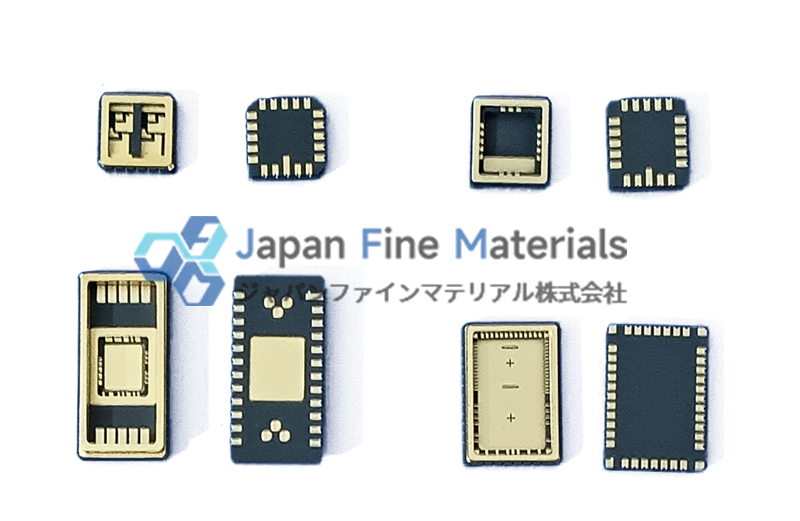
Compact structure, conducive to space utilization
With external leads removed, the CLCC package features a more regular outer contour, offering flexibility in high-density circuit design.
In practical layout, this compactness can be reflected in:
• The spacing between CLCC-packaged devices can be optimized based on pad design
• Higher package size utilization, which helps increase integration density per unit area
• Easier modular layout in multi-layer PCB designs
Furthermore, because the CLCC package profile is relatively uniform, it is easier to control during automated placement and reflow soldering processes, which is significant for mass production.
Electrical performance is easier to control
In applications involving high-frequency or high-speed signals, the CLCC package structure can affect signal transmission paths; in this regard, the CLCC package provides a relatively simplified structural foundation.
Its advantages are primarily reflected in:
• No long lead structure, which helps shorten signal paths
• Parasitic inductance and capacitance in CLCC packages are easier to estimate and control during the design phase
• Standardized pad layout rules facilitate impedance matching design
In RF or high-speed digital circuits, these factors directly impact signal integrity, and the consistency of the CLCC structure helps improve the controllability of signal paths.
Structural Consistency and Long-Term Performance
In electronic devices operating over the long term, CLCC packages must not only meet initial performance requirements but also maintain stable performance throughout their service life.
The performance of CLCC packages in this regard is typically related to the following factors:
• Minimal performance degradation of materials under long-term environmental exposure
• The CLCC package structure is not prone to significant deformation due to temperature changes
• The condition of the package interface remains relatively stable during multiple thermal cycles
These characteristics help mitigate the potential impacts of structural changes in CLCC packages, making them particularly suitable for applications that demand long-term stability.
Conclusion
CLCC packaging is best understood as a "packaging solution tailored to specific needs." Its advantages lie primarily in material stability, structural design, and adaptability to complex operating conditions, rather than serving as a replacement for all packaging types.
In practical applications, packaging selection is always part of the design trade-off. Making decisions based on specific usage scenarios is often more effective than focusing solely on a single performance metric.
If you are evaluating different packaging solutions or wish to optimize the packaging structure based on specific application conditions, CLCC can serve as a reference point for further exploration.
JFM offers a wide range of ceramic packaging products and can provide tailored support in material selection, structural design, and manufacturing to meet diverse application requirements.
Please feel free to contact our engineers to discuss packaging solutions best suited for your project.


