Key Precious Metals Used in Semiconductors Manufacturing
Overview of how key precious metals are applied in semiconductor manufacturing, including interconnects, electrodes, and thin-film processes.
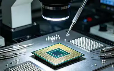
The Role of BGA Solder Ball in CSP Packaging
This article reviews the role of BGA solder balls in CSP packaging, focusing on interconnection reliability and device miniaturization.
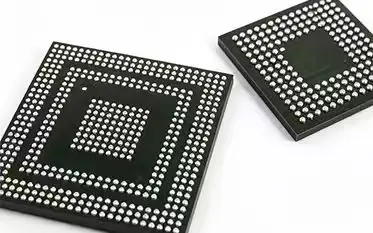
BGA Solder Ball Guide for Semiconductor Packaging
This article introduces BGA solder balls in semiconductor packaging and their role in ensuring stable chip connections, improving device reliability, and enabling compact electronic designs.
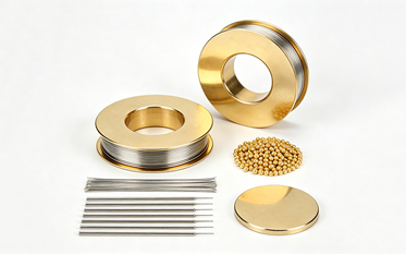
How AuSn Solder Improves Semiconductor Packaging Reliability
Learn how AuSn solder improves semiconductor packaging reliability with strong thermal conductivity, stability, and hermetic sealing performance.
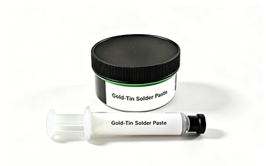
What Is Solder Paste? A Complete Guide
This guide explains solder paste in detail, including its materials, function in PCB assembly, and key process considerations in electronics manufacturing.
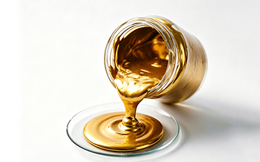
How Gold Paste Is Used in Semiconductor Packaging
Understand how gold paste is used in advanced packaging technologies and why it is important for high-reliability electronic devices.

What Is Platinum Paste Used for in Semiconductor Packaging?
Explore the function of platinum paste in modern semiconductor packaging and how it improves performance in demanding electronic environments.

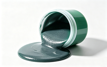
Complete Guide to the Metal Paste Manufacturing Process
Learn how metal paste is produced step by step, from metal powder selection to final testing. A practical overview for electronics and conductive material industries.
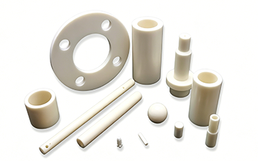
Why Alumina Ceramic Rods Are Essential in Electronics and Machinery
This article explains why alumina ceramic rods are widely used in electronics and machinery, focusing on their insulation, heat resistance, and durability in demanding operating conditions.


