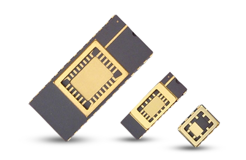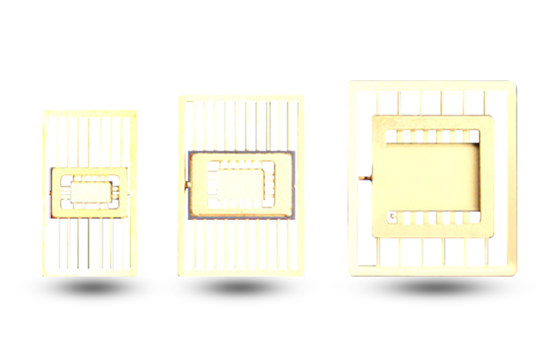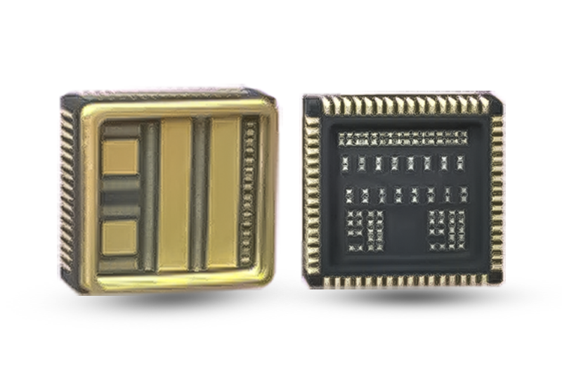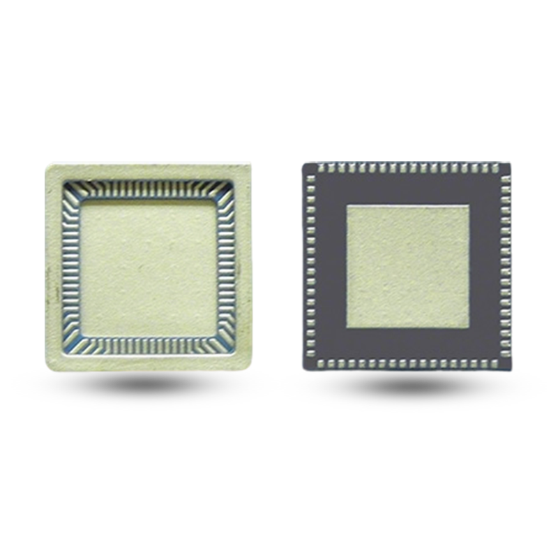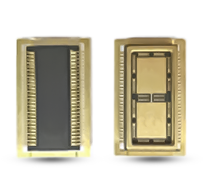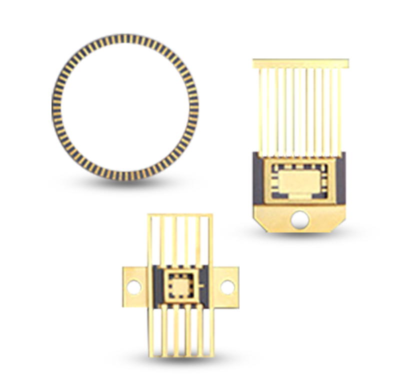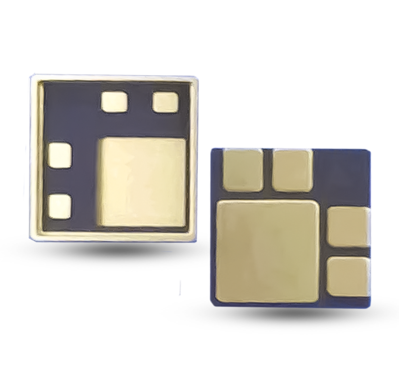
Multilayer ceramic packages, renowned for their excellent electrical properties, thermal stability, and high hermeticity, are widely utilized in the semiconductor packaging of integrated circuits (ICs), hybrid ICs, optocouplers, Hall effect devices, crystal oscillators, solid-state relays (SSRs), and discrete devices.
Leveraging our HTCC (High-Temperature Co-fired Ceramics) process, our products integrate key technologies such as Φ100μm via filling, 100μm fine-line printing, 1000mm-wide tape casting, and multi-cavity (up to 6 cavities) structural molding. We provide a comprehensive suite of supporting components, including parallel seam welding lids, AuSn (Gold-Tin) alloy solder lids, and specialized internal ceramic bases (submounts) for optocouplers. Currently, our HTCC packages for optocouplers have achieved stable mass production and supply, fully meeting the demands for high-performance and high-reliability packaging.