How Ceramic Chambers and Domes Enhance Semiconductor Manufacturing Yield
-
2026-01-16 Industry News


Ceramic chambers and domes resist extreme heat and plasma to ensure process stability. Their thermal uniformity and corrosion resistance minimize contamination, directly boosting film quality and manufacturing yield.
Introduction
In semiconductor manufacturing, yield (the rate of non-defective products) is a critical indicator for evaluating process stability, equipment reliability, and corporate profitability. As process nodes advance from 28nm to 14nm, 7nm, and beyond, the process window for wafer manufacturing has become increasingly narrow. Equipment is now facing more sophisticated requirements in terms of temperature uniformity, chemical resistance, plasma distribution uniformity, particle control, and long-term stability.
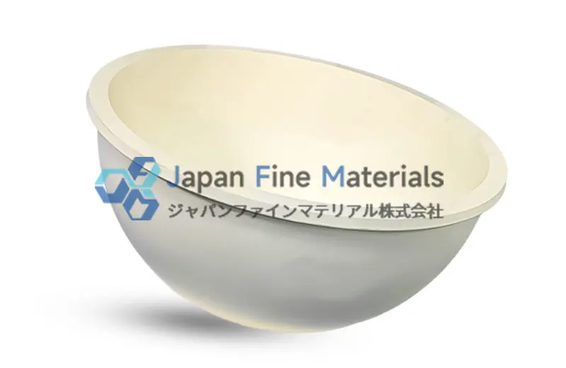
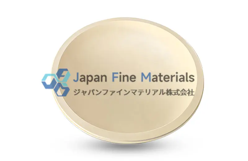
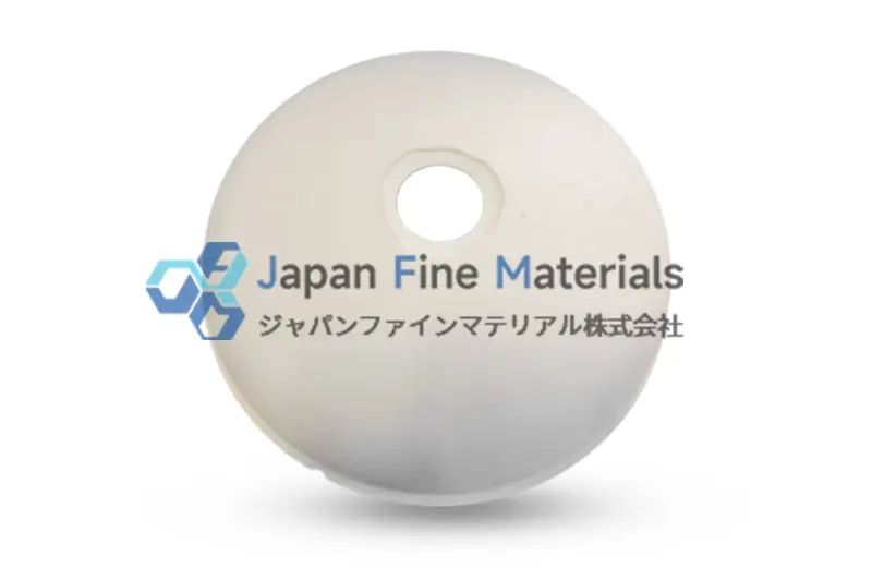
Ceramic Chambers and Domes are essential components of semiconductor equipment systems. Their material properties and structural designs directly impact wafer yield, equipment operational stability, and the continuous operation of production lines.
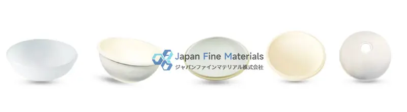
Chamber and Dome Materials
Depending on the process environment, materials are required to have high thermal stability, chemical resistance, and mechanical properties. Representative ceramic materials include:
Alumina (Al₂O₃)
● Possesses excellent heat resistance, making it suitable for process environments with repeated high-temperature cycles.
● Features a low coefficient of thermal expansion, contributing to the reduction of structural stress and deformation caused by temperature changes.
● Offers superior mechanical strength and rigidity, with high resistance to micro-cracks.
 |
 |
 |
Quartz
● Exhibits excellent chemical inertness, resisting corrosion from strong acids, strong alkalis, and plasma.
● Features a low coefficient of thermal expansion and minimal thermal stress.
● Offers superior translucency and electrical insulation, suitable for lithography, PECVD, and specific deposition processes requiring particular optical or electrical properties.
● The adoption of high-purity, high-performance materials stabilizes the temperature field and reduces particle generation.
This contributes to extending equipment lifespan, improving wafer yield, and reducing process loss and rework rates.
Thermal Field Uniformity Design
Wafers are highly sensitive to temperature gradients in high-temperature processes. Even slight temperature differences can lead to non-uniform film thickness, localized concentration of internal material stress, or the formation of micro-cracks. By optimizing the chamber wall thickness, angles, and opening layouts, and combining materials with stable thermal expansion characteristics such as high-purity alumina or silicon nitride (Si₃N₄), the temperature difference across the wafer surface can be reduced, ensuring thin-film uniformity.
Thermal simulations based on Finite Element Analysis (FEA) are effective for evaluating heat flux paths and temperature distribution characteristics within the chamber, providing guidelines for structural design and material selection. Achieving a uniform thermal field not only mitigates the adverse effects of thermal stress on the chamber structure and wafer but also helps maintain process stability and repeatability during continuous high-temperature cycles.
Plasma Field Optimization
Non-uniform plasma distribution can induce micro-loading effects during etching and deposition processes, leading to variations in film thickness, inconsistent etching results, or an increase in wafer surface defects. By optimizing the chamber shape, wall thickness, and the dielectric properties of the ceramic materials used, the electromagnetic field distribution within the chamber can be controlled, contributing to a more uniform plasma density distribution and suppressing localized power concentration.
Furthermore, combining electromagnetic field simulations with ion density calculations enables chamber designs tailored to specific combinations of power, frequency, and process gases. Stabilizing the plasma distribution improves etching precision, deposition uniformity, and process repeatability, ultimately having a positive impact on wafer yield and surface quality.
Particle Generation and Contamination Control
Particle contamination is a major factor affecting wafer yield. By employing high-density ceramic materials and applying precision surface polishing, the occurrence of micro-cracks and pores can be suppressed, reducing particle generation. Additionally, combining corrosion-resistant coatings or wear-resistant treatments further inhibits particle shedding, contributing to extended chamber life and the maintenance of cleanliness in the production environment.
The design of gas flow within the chamber is also critical. Optimizing the layout of gas flow paths, gas outlet positions, and velocity distribution allows for control over particle suspension behavior and the tendency for particles to adhere to the wafer surface. Advancements in particle control not only reduce contamination risks but are also effective in maintaining deposition uniformity, contributing to consistent wafer processing and improved process yield.
Modularization and Process-Compatible Design
Modular design allows for rapid installation, removal, cleaning, and replacement of the chamber, significantly reducing equipment downtime and process variability. By integrating the optimization of thermal fields, electric fields, and particle control, modular structures demonstrate high adaptability to different equipment models and process environments, contributing to reductions in custom development time and operational costs.
A modularized chamber structure improves maintainability and makes it easier to maintain a relatively stable processing environment even during long-term operation. Through multi-faceted collaborative optimization, it supports the stable maintenance of wafer yield, continuous production line operability, and process reliability, ensuring the performance required for advanced semiconductor manufacturing based on quantitative metrics.
Precision Manufacturing Process
The manufacturing process of ceramic chambers and domes is a critical factor determining stability and reliability during long-term operation. A high-precision manufacturing flow not only contributes to maintaining consistency in chamber dimensions, structure, and material properties but is also effective in extending equipment lifespan, reducing particle generation, and improving wafer yield. Every step, from raw material preparation to final inspection, is strictly managed to ensure compliance with the high quality standards required for industrial applications.
JFM's key processes and features are as follows:
1. High-Precision Forming
● A combination of several methods is applied, including CNC precision machining, mold press forming, and injection molding.
● Excellent capability in managing dimensional tolerances ensures high-precision fitting between the chamber and equipment interfaces, contributing to reduced misalignment during installation.
2. High-Temperature Sintering and Densification
● A multi-stage sintering process promotes densification within the ceramics.
● Suppresses the occurrence of micro-cracks and ensures high mechanical strength.
● Enhances thermal stability, making the parts suitable for use under conditions involving high-temperature cycles and thermal shock.
3. Surface Treatment and Coating
● Precision polishing reduces surface roughness and is effective in suppressing particle shedding.
● Corrosion-resistant coatings can be selected to improve durability in specific chemical environments.
● Increases compatibility with plasma processes, contributing to uniform etching and deposition.
4. Inspection and Traceability
● Multi-faceted inspection items are established, including dimensional accuracy, density, thermal expansion characteristics, mechanical strength, and chemical resistance.
● Traceability at the product unit level supports the maintenance of long-term process consistency.
● Systematic quality control reduces defect rates during the manufacturing process.
5. Comprehensive Synergies
● A coordinated system is established that links forming, sintering, surface treatment, and inspection.
● Contributes to the stable maintenance of ceramic chamber/dome structures and properties even under harsh process environments such as high temperatures, high energy, and strong corrosion.
● Forms a comprehensive technical approach aimed at improving yield in coordination with design optimization and material selection.
Through this manufacturing process system, ceramic chambers and domes easily maintain high performance stability even under severe semiconductor process conditions. They not only provide structural support for the wafer manufacturing process but also contribute to extending equipment maintenance cycles, maintaining continuous production line operability, and improving process reliability.
Why Choose JFM's High-Purity Precision Ceramic Components?
As a company that integrates R&D and manufacturing of industrial ceramics, JFM has accumulated years of technical expertise in the field of ceramic components for semiconductors.
● Material Strengths: Employs high-purity ceramic materials to achieve excellent heat resistance, chemical corrosion resistance, and low thermal expansion characteristics.
● Design Strengths: Comprehensively considers thermal field distribution, electric field compatibility, and particle control, while also meeting implementation needs through modularization.
● Manufacturing Collaboration: Based on JFM's industry-proven manufacturing standards, we collaborate with partners experienced in semiconductor ceramic production to implement high-precision forming, high-temperature sintering, surface polishing, and inspection, ensuring quality that meets the required specifications of advanced process equipment.
● Application Suitability: Widely adopted in wafer manufacturing equipment supporting 28nm, 14nm, and subsequent advanced nodes.
● Custom Capabilities: Provides custom solutions for high-purity precision ceramic components suited to the operating conditions of various fields, including semiconductors, flat panel displays, petrochemicals, energy, medical devices, industrial machinery, and electronics/telecommunications.
If you are considering custom ceramic chambers, domes, or various functional ceramic components for high-vacuum environments, PVD, CVD, or plasma etching equipment, please contact JFM. We will propose the optimal custom ceramic solution based on your engineering requirements.


