Custom Alumina Ceramic Components for Semiconductor Applications
-
2026-03-09 Industry News


Custom Alumina components for semiconductor tools. High-purity Al2O3 offers superior plasma resistance and thermal stability for wafer handling and etching.
1. Introduction
With outstanding physical and chemical properties, alumina ceramics have become an essential foundational material in the semiconductor industry. Even under demanding environments such as high temperatures, strong corrosion, and cleanroom conditions, alumina ceramics maintain superior insulation, mechanical strength, and corrosion resistance, providing stable and reliable support for semiconductor equipment. Customized ceramic components are widely utilized in plasma etching, wafer handling, vacuum systems, and testing equipment, successfully translating material characteristics into device performance.
2. Basic Properties of Alumina Ceramics
High-Temperature Stability
Alumina ceramics maintain structural stability at temperatures exceeding 1400°C. Due to their low coefficient of thermal expansion, they are suitable for critical components in high-temperature semiconductor equipment, including plasma etching systems, Chemical Vapor Deposition (CVD), and Atomic Layer Deposition (ALD). This thermal stability reduces component cracking or deformation during repeated thermal cycling, extending equipment service life.
Superior Insulation and Low Dielectric Loss
Characterized by high dielectric strength and low dielectric loss, these ceramics are ideal for wafer positioning supports, ceramic insulation rings, electrostatic chucks, and high-frequency electrical applications. Stable insulation performance effectively prevents discharge and signal interference, ensuring the precision and reliability of semiconductor manufacturing processes.
High Hardness and Wear Resistance
Alumina ceramics feature high hardness and a low friction coefficient, making them suitable for moving parts such as guide rings, sliding rail components, and support blocks. Superior wear resistance not only reduces mechanical wear but also minimizes particle generation, ensuring the cleanliness of cleanroom process environments.
Corrosion Resistance
Dense ceramic surfaces withstand erosion from highly corrosive plasmas and chemical reagents such as Cl₂, F₂, and O₂. Compared to metal components, alumina ceramics offer higher resistance to chemical corrosion in both wet and dry semiconductor processes, extending the lifespan of critical parts and reducing maintenance frequency.
Highly Customizable
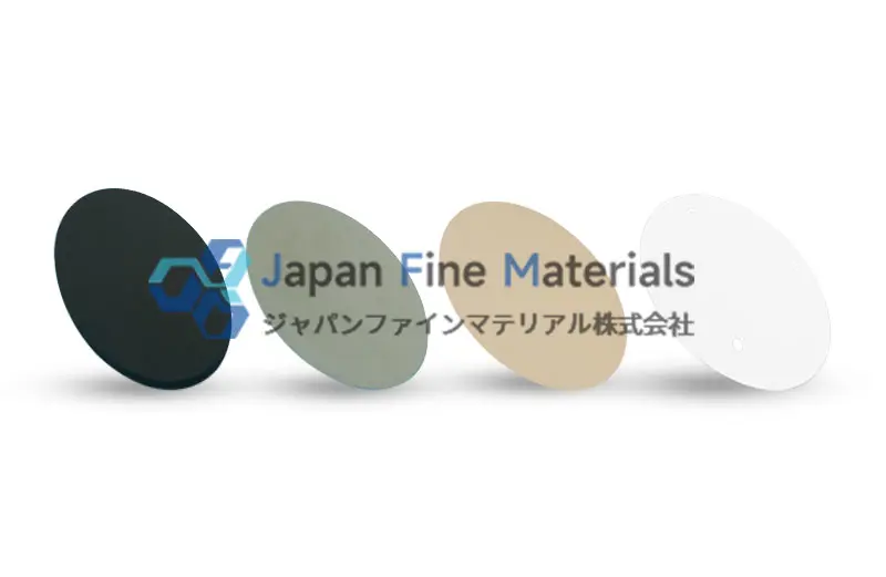
Alumina ceramics can be customized in terms of size, shape, hole configuration, mounting methods, and surface precision to meet equipment structural requirements. Customized designs address the needs for complex structural parts, micro-hole machining, and high-precision fitting, maximizing material properties to enhance equipment performance.
3. Plasma Etching and High-Temperature Chamber Components
Alumina ceramics are primary materials for chamber structures and electrode supports in semiconductor plasma etching and high-temperature CVD/ALD systems. Capable of withstanding temperatures over 1400°C, they also feature a low thermal expansion coefficient and high thermal conductivity, ensuring structural stability during rapid heating and cooling cycles. High-purity (99% to 99.8%) alumina ceramics provide excellent insulation and low dielectric loss, effectively supporting high-voltage electrode holders and electrostatic chucks while reducing electrical interference and particle contamination.
Typical Components and Functions:
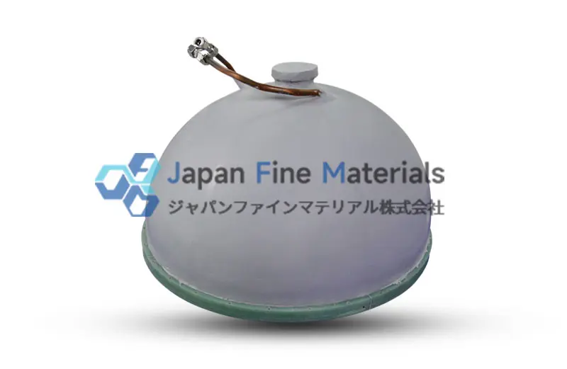
● Ceramic Dome: High-temperature resistance and high-density structure ensure the stability of the entire chamber.
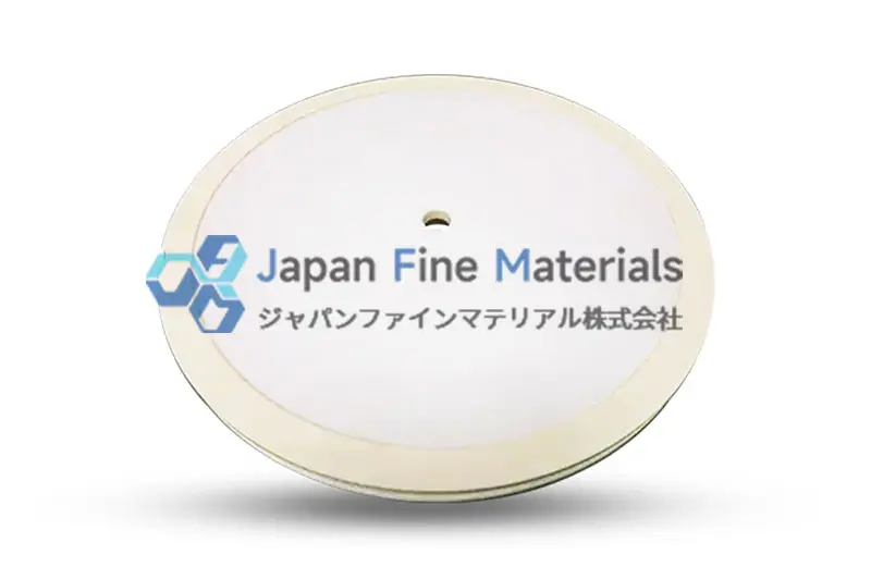
● Ceramic Window: Corrosion and high-temperature resistant, suitable for chamber observation and optical inspection.
● Ceramic Insulator: High insulation and low dielectric loss for electrode supports, electrostatic chuck pillars, blocks, and insulating parts.
 |
 |
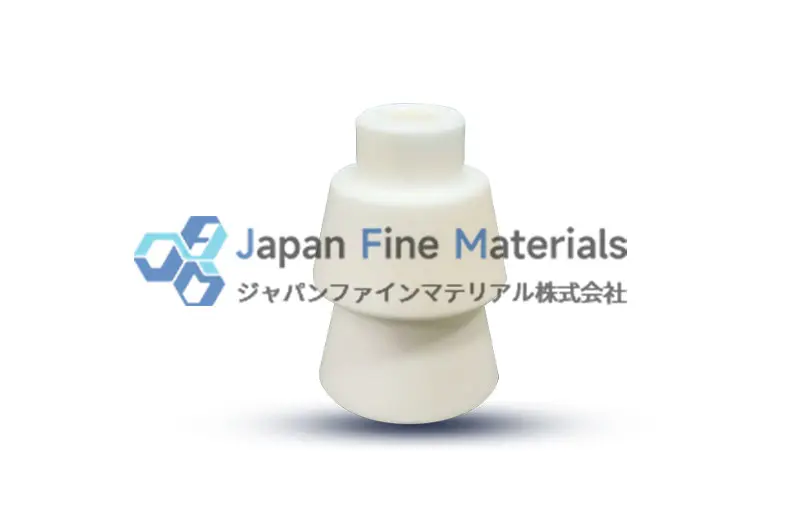 |
| Ceramic Dome | Ceramic Window | Insulating Tube |
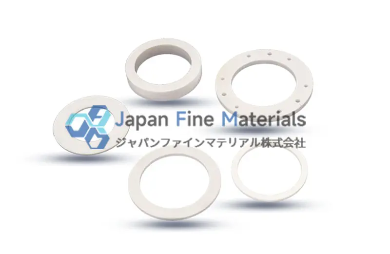
4. Wafer Handling and Support Components
In wafer handling systems, components require extremely high wear resistance, dimensional stability, and precision. Alumina ceramic arms withstand mechanical friction and plasma corrosion, ensuring accurate wafer transport. Ceramic rings acting as wafer guides and supports combine corrosion resistance with high-temperature stability. Ceramic vacuum chucks provide high thermal insulation and wear resistance, ensuring secure wafer retention during handling. Custom designs are available for various wafer sizes and equipment requirements, including arm length, chuck apertures, and ring dimensions.
Typical Components and Functions:
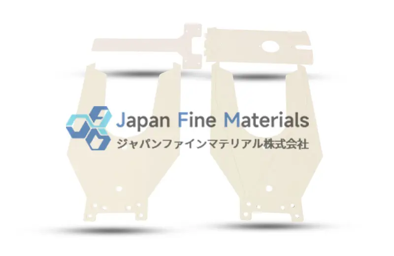
● Ceramic Arm (End Effector): Wear and corrosion resistant, supporting precise handling.
● Ceramic Ring: Provides wafer positioning and guide support in high-temperature plasma environments.
● Ceramic Vacuum Chuck: High thermal insulation and wear resistance ensure handling precision.
 |
 |
 |
| Ceramic Arm | Ceramic Ring | Vacuum Chuck |
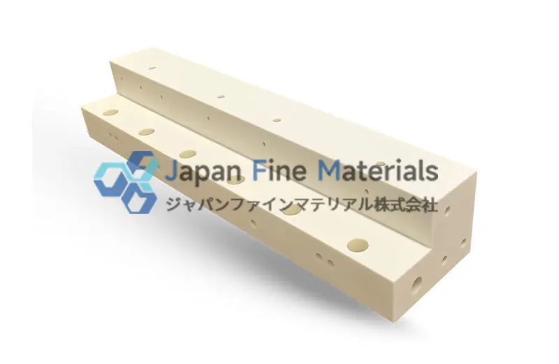
5. Guide and Motion Components
Wafer transport and mechanical sliding components require materials with high hardness, low friction, and long-term wear resistance. Alumina ceramic guides operate stably under harsh conditions such as wet cleaning or plasma etching. High-density materials ensure mechanical precision, while low porosity minimizes particle generation. Guide surface flatness and geometric accuracy directly impact wafer movement stability. Customized lengths, widths, and groove shapes ensure precise alignment with wafer trays or robotic arms.
Typical Components and Functions:
● Ceramic Guide Rail: Features high hardness, wear resistance, corrosion resistance, and high-temperature stability.
● Customization Options: Flexible length, width, groove geometry, and surface roughness.
 |
| Ceramic Guide Rail |
6. Gas Flow and Process Control Components
Alumina ceramics are used in etching, deposition, and cleaning equipment to precisely control reactive gas flow and ensure process stability. Ceramic nozzles feature high density, corrosion resistance, and heat resistance. Their low thermal expansion coefficient ensures stable orifice shapes during long-term use. Customized designs for orifice diameter, angle, and distribution optimize airflow uniformity, reducing edge effects and improving process stability. Surface finish and porosity are critical parameters for minimizing particle generation and gas turbulence.
Typical Components and Functions:
● Ceramic Nozzle: Provides stable flow with superior corrosion and high-temperature resistance.
● Customization Options: Optimization of aperture, shape, and layout.
 |
| Ceramic Nozzle |
7. CMP and Surface Treatment Components
In the Chemical Mechanical Planarization (CMP) process, alumina ceramic components play a vital role in pressure transmission. Polishing pads made of high-hardness, wear-resistant ceramics ensure wafer surface flatness and polishing uniformity. This material is chemically resistant and adaptable to various polishing slurries and cleaning solutions. Design considerations include flatness, thickness uniformity, and surface roughness. Diameter, thickness, and mounting structures can be customized to match specific equipment requirements.
Typical Components and Functions:
● Polishing Pad: Achieves uniform pressure distribution and ensures wafer flatness.
● Customization Options: Diameter, thickness, and fixing structure.
 |
| Ceramic Polishing Disc |
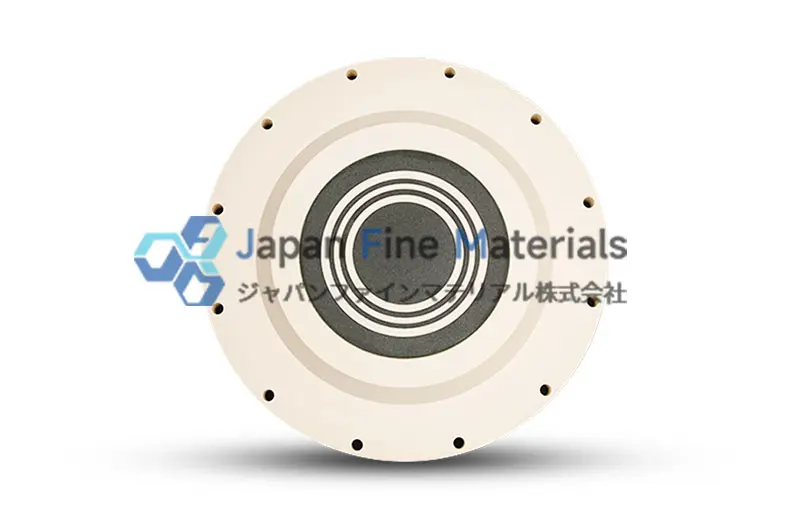
8. Electronic Substrates and Processing Platform Components
Alumina ceramic substrates are widely used as support materials for wafers and chips in semiconductor testing and packaging equipment. These substrates feature high insulation, thermal stability, and mechanical strength, withstanding prolonged heating and cooling cycles without deformation. Customized designs for hole layout, thickness, and surface finish meet precise positioning and electrical signal isolation needs. High-purity materials (99% to 99.8%) minimize particle contamination, ensuring wafer safety and process stability during testing and packaging.
Typical Components and Functions:
● Ceramic Substrate: High insulation, thermal stability, and mechanical strength.
● Customization Options: Hole layout, thickness, and surface treatment.
 |
| Ceramic Substrate |
9. Key Values of Customized Alumina Ceramic Components
Providing a Structural Foundation for Process Stability
Alumina ceramics exhibit exceptional dimensional stability even in high-temperature and vacuum environments. Ceramic supports, insulation rings, and positioning parts maintain an accurate fit during long-term operation, reducing the risk of structural displacement due to thermal deformation.
Ensuring Electrical Safety and Process Consistency
With superior electrical insulation, alumina ceramics are widely used in high-voltage and high-frequency regions. They ensure stable equipment operation under complex conditions, preventing electrical interference from affecting the manufacturing process.
Extending the Lifespan of Consumable Parts
In plasma etching and chemical processing environments, the dense structure and chemical stability of alumina ceramics effectively enhance the corrosion resistance of chamber protectors, baffles, and isolation parts, significantly reducing replacement frequency and maintenance costs.
Reducing Overall Equipment Operation and Maintenance Costs
By using alumina ceramic components in critical areas, semiconductor equipment can maintain stable operation over long periods, reducing unexpected downtime and improving overall production efficiency.
10. Conclusion
As semiconductor manufacturing processes evolve toward higher precision and stability, material properties have become a key factor determining equipment reliability. Alumina ceramics, with their combined advantages of high-temperature resistance, superior insulation, and plasma corrosion resistance, have transitioned from "general structural materials" to critical functional materials in semiconductor equipment. Customizing ceramic components to precisely tune material properties for specific equipment structures and process environments has become an industry standard.
Why Choose JFM Alumina Ceramics?
We do more than just provide ceramic parts; we help translate material characteristics into improved equipment stability and lifespan through an engineering approach that considers equipment structure, process conditions, and usage environments.
● Multiple alumina purity levels are available to suit various semiconductor process environments.
● Support for customized structures and dimensions to meet installation and precision requirements.
● Stable precision machining capabilities suitable for long-term use of critical ceramic parts.
● Strict quality control ensures batch consistency and reliability.
If you are seeking a reliable partner for custom alumina ceramic components for semiconductor equipment, please contact JFM. Our engineering team provides professional advice and customized support based on your equipment structure and process requirements, helping improve stability and reduce overall operating costs.


