What are ceramic packages in semiconductor applications?
-
2026-03-06 Industry News


Ceramic packages ensure electrical and thermal stability for chips. Using Alumina, AlN, and Si3N4, they offer heat resistance and reliability for power and RF devices.
1. Introduction
As semiconductor devices evolve toward high power, miniaturization, and complex operating environments, industry discussions often focus on process nodes, chip architectures, or material innovations. However, in practical applications, many device failures do not originate from the chip itself, but from "packaging"—a factor that is sometimes underestimated.
Packaging determines the connection between the chip and external systems and directly affects the long-term stability of the device under high temperatures, thermal cycling, mechanical stress, and high-humidity environments. As operating conditions move beyond the standard range of consumer electronics, the limitations of traditional plastic packaging solutions are becoming more apparent.
Against this backdrop, ceramic packages are regaining importance in semiconductor applications. Ceramic packaging is designed as an engineering choice focused on reliability, thermal management, and structural stability. In power semiconductors, automotive electronics, and other high-reliability applications, ceramic packaging is often an essential component of system design.
2. What Role Does Ceramic Packaging Play in Semiconductors?
In semiconductor devices, ceramic packages serve as more than an outer shell; they are critical components that ensure chip performance, reliability, and lifespan. Specifically, they fulfill several key roles:
Mechanical Support and Protection
Chips are fragile, especially high-pin-count, high-power, or large-scale chips where slight vibrations or stress can lead to cracks or wire bonding failures. Ceramic packages provide stable mechanical support through robust ceramic substrates and precise structural designs, protecting the chip from external impact.
Electrical Interface and Signal Transmission
Chip electrodes must be reliably connected to external circuits. Ceramic packages feature metallized traces or pads to achieve high-precision electrical interfaces. In radio frequency (RF), high-speed signal, or high-power applications, the internal circuit design of the package affects signal integrity, parasitic inductance, and capacitance, which influences device performance.
Thermal Management and Heat Dissipation
High-output devices generate heat during operation. If this heat is not dissipated, efficiency decreases, potentially leading to failure. Ceramic materials possess high thermal conductivity. When combined with optimized package structures, they conduct heat to external cooling systems, protecting the chip and supporting stable operation.
Environmental Isolation and Hermetic Protection
Ceramic packages enable hermetic sealing, isolating the chip from moisture, oxides, corrosive gases, and other contaminants. This is vital for high-reliability applications in semiconductors, automotive electronics, and medical devices, as environmental factors are primary causes of premature chip failure.
Stress Mitigation and Matching
Temperature changes and mechanical stress can cause thermal expansion mismatches between the chip and the package. By selecting appropriate materials and optimizing structural design, ceramic packages reduce the impact of thermal stress on the chip, enhancing reliability.
Support for High-Pin-Density Design
Modern semiconductor devices require more pins, higher integration, and multi-layer wiring. Ceramic packages accommodate multi-layer circuits, metal vias, and complex internal structures, providing suitable packaging solutions for high-performance chips.
3. Why is Ceramic Chosen Over Plastic in Semiconductors?
While plastic packaging is prevalent, the requirements for specialized semiconductor applications are different. Ceramic materials offer properties that plastic cannot provide:
● High temperature resistance allows for operation in harsh environments.
● A stable Coefficient of Thermal Expansion (CTE) enables matching with silicon chips.
● High thermal conductivity aids in the heat dissipation of power devices.
● Electrical insulation properties remain stable over time.
● Provides reliable hermetic sealing.
Packaging remains a preferred choice for power semiconductors and medical electronics.
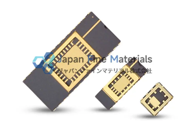
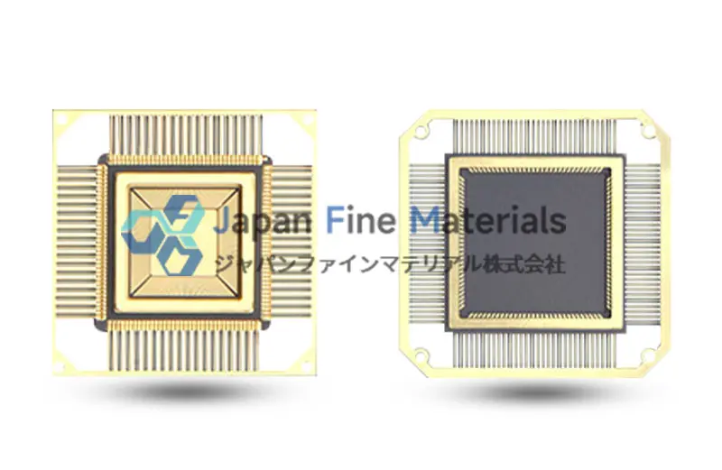
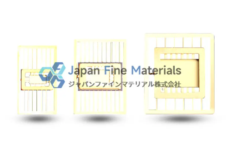
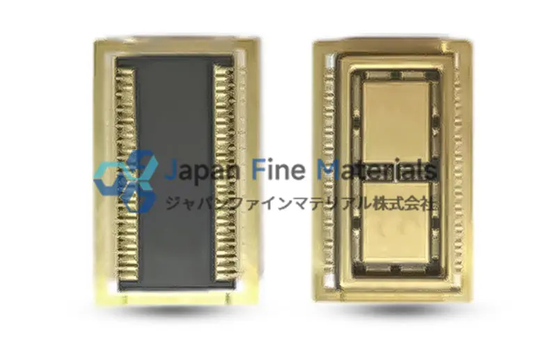
4. Common Ceramic Packaging Formats
In semiconductor applications, ceramic packages come in various designs depending on the chip type and application scenario. Each offers advantages in structure, pin layout, and thermal management. Common types include:
CDIP (Ceramic Dual In-Line Package)
Suitable for chips with low to medium pin counts. Ceramic materials provide thermal stability, mechanical strength, and hermeticity, making them appropriate for high-reliability applications.
Suitable for multi-pin processors and memory chips. The ceramic structure ensures heat dissipation and mechanical stability, withstanding repeated insertion and removal while meeting reliability requirements.
CQFP (Ceramic Quad Flat Package)
Used for ICs with medium to high pin counts. Ceramic materials maintain electrical performance and mechanical strength during operation, making them suitable for complex signal processing devices.
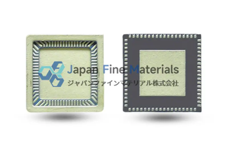
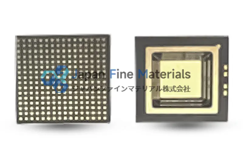
CLCC (Ceramic Leadless Chip Carrier)
Appropriate for small-footprint, high-density packaging requirements. Features a compact structure, short signal paths, and stable electrical performance, ideal for high-frequency electronic modules.
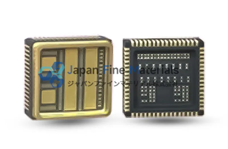
CQFN (Ceramic Quad Flat No-Lead)
Used in power ICs and RF devices for its compact design and heat dissipation properties, providing reliable performance within limited space.
Features a small package area, suitable for compact power ICs and modules, particularly in applications with thermal management needs.
CSOP (Ceramic Small Outline Package)
A compact surface-mount housing offering mechanical impact resistance, hermeticity, and moisture resistance. Used for memory, integrated circuits, and relays.
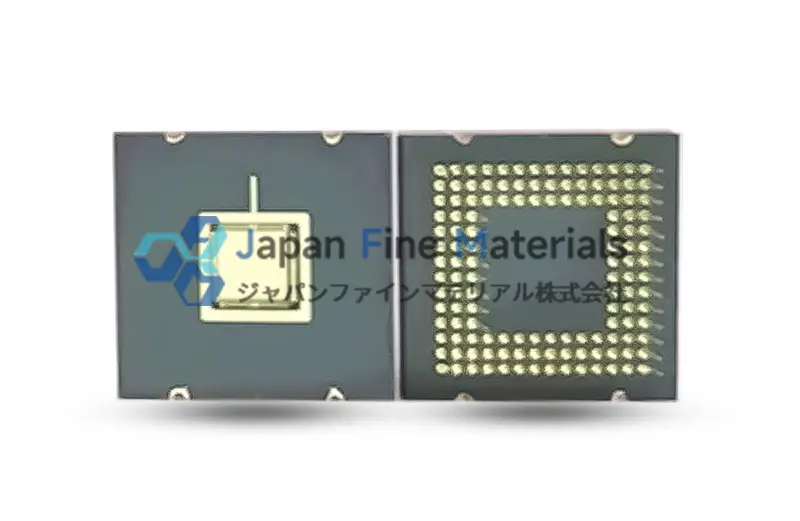
CLGA (Ceramic Land Grid Array)
Used for chips such as microprocessors and CPUs. Its density layout and hermetic sealing make it suitable for high-end sensors, ASICs, and discrete modules.
In addition to standard types, customized designs—including pin layouts and material selections—are available to meet specialized application scenarios and reliability standards.
5. Common Ceramic Packaging Material Types
In semiconductor ceramic packaging, different materials offer varying characteristics regarding reliability and heat dissipation. Selecting the appropriate ceramic ensures stable device operation.
| Material | Features and Applications |
|---|---|
| Alumina (Al2O3) | Balanced cost and stable performance; suitable for industrial control and general power chip packaging. |
| Aluminum Nitride (AlN) | High thermal performance; ideal for high-power, high-density device dissipation requirements. |
| Silicon Carbide (SiC) | High strength and heat resistance; suited for complex operating conditions and power modules. |
| Zirconia (ZrO2) | High hardness and strength; suitable for wear-resistant encapsulation needs. |
Material selection must consider device power, operating environment, and reliability needs to enhance the service life of the package.
6. Key Application Scenarios for Ceramic Packaging
In the current market, ceramic packaging is used in semiconductor applications requiring performance and reliability.
● Power semiconductor modules (IGBT, SiC, GaN) used in high-current applications.
● Automotive electronics, such as electric vehicle inverters and control units.
● RF, microwave, and communication devices with requirements for signal integrity and thermal stability.
● Medical devices and sensors requiring stable operation.
In semiconductor systems, packaging is a component that influences device longevity. Ceramic packaging is utilized because it provides stable engineering performance in high-temperature and high-power contexts.
If you are evaluating packaging solutions or custom ceramic designs, please contact us. We provide guidance on material selection and structural design based on your application.
7. Frequently Asked Questions
1) Is ceramic encapsulation always superior to plastic encapsulation?
Not necessarily. Ceramic packaging is a solution for different requirements. While plastic is used for mass-produced consumer goods, ceramic offers advantages in stability for high-power or high-temperature applications.
2) When is ceramic encapsulation necessary?
Ceramic packaging is a choice when devices must withstand thermal cycling, high power density, or require hermetic sealing, such as in power semiconductors.
3) Why is ceramic packaging more expensive?
The cost is related to the materials, the complexity of the sintering and metallization processes, and quality control. It is generally utilized where performance and reliability are required.
4) Do ceramic packages support custom designs?
Yes, this is an advantage. Substrate structures, metallized circuits, and the package itself can be customized based on chip size and operating environment.
5) Is ceramic packaging effective for heat dissipation?
Yes, with appropriate materials. For example, Aluminum Nitride offers thermal conductivity higher than alumina or plastic, meeting the needs of high-power devices.
6) Will ceramic packaging be replaced by newer technologies?
Unlikely in the near term. Many new packaging technologies incorporate ceramic materials into their substrates or structures to maintain reliability and power handling.


