Common Types of Ceramic Packages: A Design and Application Guide
-
2026-04-03 Industry News


Explore common types of ceramic packages, including CLCC, CDIP, CQFP, and CSOP. Learn their design features, performance advantages, and key applications across semiconductor, medical, and industrial fields.
Introduction
With the advancement of electronic packaging technology, ceramic materials have been widely adopted in the packaging of various electronic devices due to their performance in thermal conductivity, structural stability, and environmental adaptability. Depending on circuit complexity and assembly methods, ceramic packaging has evolved into a variety of structural types. Understanding these common types and their design differences helps in making more appropriate selection decisions for projects.
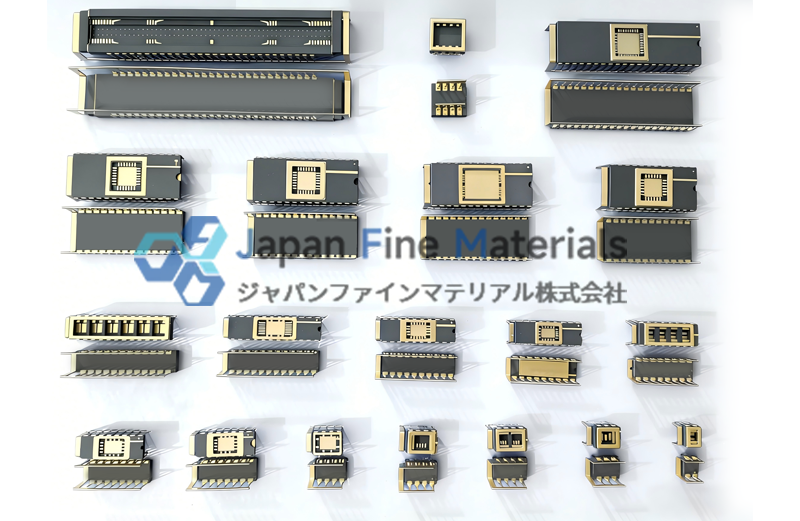
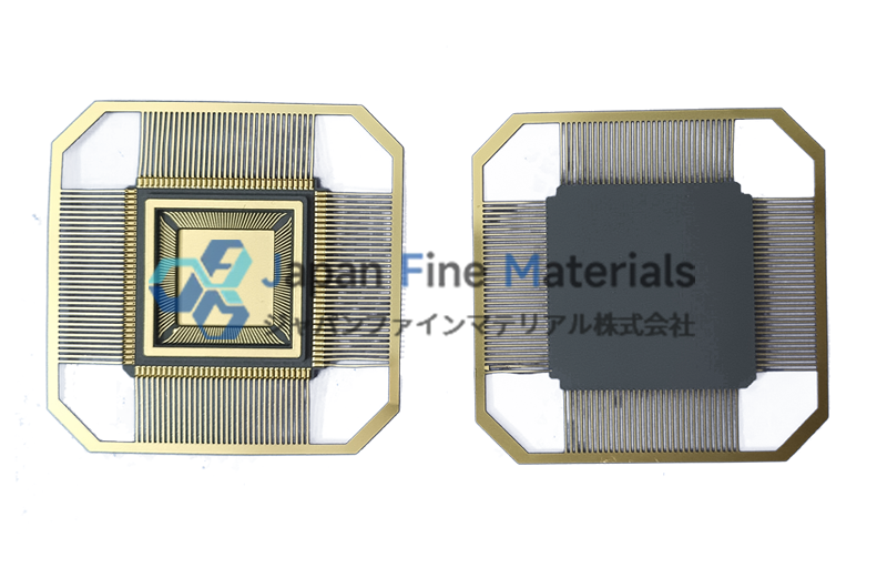
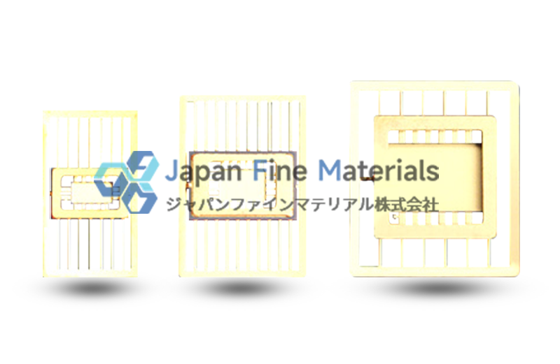
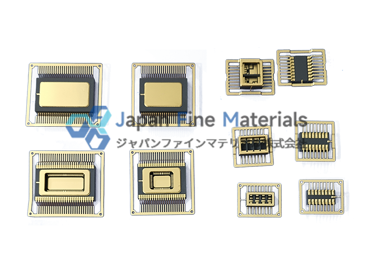
Basic Structure of Ceramic Packages
Ceramic packages typically use materials such as aluminum oxide (Al₂O₃) or aluminum nitride (AlN) as substrate materials. Through a series of microelectronic packaging processes, the chip, circuitry, and external connection structures are integrated into a relatively stable packaging system. Compared to common plastic packages, ceramic materials possess distinct characteristics in terms of thermal conductivity, dimensional stability, and adaptability to environmental changes; therefore, they are more frequently selected in scenarios where high packaging performance is required.
Structurally, a complete ceramic package typically consists of the following key components:
• Chip mounting: Securing the chip to the ceramic substrate or inside the cavity while ensuring the establishment of thermal pathways
• Wire bonding (gold wire/aluminum wire): Used to establish electrical connections between the chip and external circuits
• Metallization layers: Forming conductive paths on the ceramic surface to connect internal structures with external interfaces
• External connection structures: Leads, pads, or balls, which serve to connect to the PCB depending on the package type
• Capping or hermetic sealing: Used in certain designs to isolate the internal device from the external environment
The differences between various package types essentially center on the form of external connections, internal layout methods, and the overall structural design logic. For example, leaded packages place greater emphasis on connection flexibility, while leadless or array-type packages focus more on space utilization and routing efficiency.
Pin-type ceramic packages
This type of package establishes a connection with the PCB via external metal leads. The leads form a structural transition zone that helps distribute stress during the assembly process. In certain through-hole or mixed-assembly scenarios, this structure still holds practical value.
Ceramic Dual In-Line Package (CDIP)
CDIP features a dual-row pin design, with pins distributed on both sides of the package. Its uniform structure facilitates standardized layout on the PCB. In through-hole mounting processes, this package type integrates more easily with existing production workflows.
CDIP is more suitable for circuit modules with relatively independent functions. In systems requiring a certain degree of serviceability, this structure also facilitates replacement and adjustment.
Key Features:
• Dual-in-line pin structure
• Compatible with through-hole mounting processes
• Clear layout, facilitating maintenance
Ceramic Quad Flat Package (CQFP)
The CQFP distributes pins around the perimeter of the package, allowing for an increased number of pins while maintaining a relatively compact form factor. This structure is commonly used in surface-mount technology (SMT) and is suitable for circuit designs of moderate complexity.
CQFP is typically used for modules requiring a certain number of I/O pins, striking a balance between size and functionality.
Key Features:
• Four-sided pin layout
• Supports SMT mounting
• Suitable for circuits of moderate integration
Ceramic Flat Package (CFP)
CFP emphasizes a flat package design, with pins distributed on two sides or all four sides, making it easier to control the overall height. In space-constrained devices, this structure integrates more easily with the overall system layout.
CFP is commonly used in electronic modules with specific structural size requirements, helping to enhance the overall compactness of the design.
Key Features:
• Flat structure, reduced height
• Flexible pin layout
• Suitable for compact devices
Ceramic Small Outline Package (CSOP)
The CSOP excels in size control, featuring a compact package volume and tight pin spacing, making it ideal for PCB designs with limited space. Additionally, this package type is well-suited for automated placement processes.
CSOP is better suited for miniaturized electronic products, helping to achieve higher functional density within limited space.
Key Features:
• Small-size package
• Compact pin pitch
• Suitable for automated production
Leadless ceramic package
Leadless ceramic packages achieve connections via bottom pads or contact areas, reducing the space occupied by external leads. This type of structure is better suited for high-density PCB designs and is also easier to integrate into automated placement processes.
Ceramic Leadless Chip Carrier (CLCC)
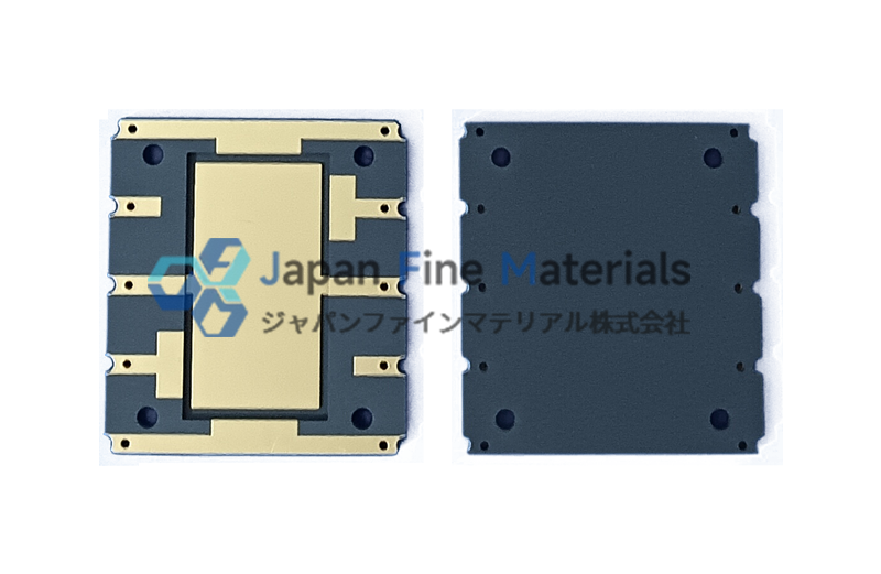
CLCC eliminates exposed leads and connects via the package edges or bottom pads, resulting in a more compact overall structure. In high-density circuits, this package helps improve space utilization.
During design, the layout of the pads must be coordinated with placement accuracy to ensure connection reliability.
Key Features:
• Leadless design
• Pads distributed along the edges or on the bottom
• Compact package
Ceramic Quad Flat No-Lead Package (CQFN)
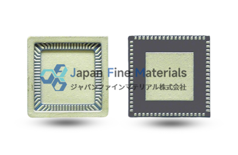
CQFNs achieve connectivity via bottom pads, reducing the package’s outer dimensions and allowing devices to be arranged more densely on the PCB. This structure is commonly found in highly integrated circuits.
During application, overall considerations must be made regarding both the soldering process and thermal path design.
Key Features:
• Bottom pad connection
• No exposed leads
• Suitable for high-density layouts
Ceramic Land Grid Array (CLGA)
The CLGA features an array of pads that provide electrical connections through multiple contact points. This structure is suitable for circuit systems requiring a large number of pins and helps increase connection density.
During the design process, PCB routing must be carefully planned to accommodate its array structure.
Key Features:
• Arrayed pad layout
• Multi-point connection method
• Supports SMT mounting
Array-pin ceramic package
This type of package uses an array of pins for connections. Compared to linear pin structures, it offers greater flexibility in expanding the number of pins and is suitable for complex circuit systems.
Ceramic Pin Grid Array (CPGA)
CPGA uses an arrayed pin layout, supporting a greater number of connection paths. This packaging type is commonly used in circuits with high demands for multi-signal processing or data exchange.
In practical design, sufficient space must be reserved for the pin array to ensure proper routing.
Key Features:
• Array Pin Structure
• Supports a large number of connection points
• Suitable for complex circuits
From a structural perspective, the differences among various ceramic package types primarily revolve around leaded connections, leadless mounting, and array structures. In practical applications, a comprehensive evaluation of circuit complexity, PCB space, and assembly methods is typically required to select the most suitable packaging solution.
Why Choose Ceramic Packaging Over Plastic
During the selection process for electronic packaging, both ceramic and plastic packages are typically considered. There are differences between the two in terms of material composition, structural performance, and applicable scenarios, so each has its own specific applications in different projects.
From a material perspective, ceramic packages primarily use inorganic materials such as aluminum oxide (Al₂O₃) or aluminum nitride (AlN), which offer a balanced performance in terms of thermal conductivity and structural stability; plastic packages, on the other hand, are typically based on epoxy resin systems and are better suited for applications focused on standardized production and cost control.
In terms of structural performance, ceramic packaging exhibits relatively controlled dimensional changes under fluctuating temperatures, which helps maintain the stability of the packaging structure; plastic packaging performs well under standard operating conditions but may rely more heavily on specific design and process support in complex environments.
|
VS |
Ceramic Packaging |
Plastic Packaging |
|
Material Type |
Inorganic materials such as alumina and aluminum nitride |
Organic materials such as epoxy resin |
|
Thermal Conductivity |
Relatively more conducive to heat conduction |
Heat dissipation through structural design |
|
Structural Stability |
Performs relatively stably under temperature fluctuations |
Performs well under normal conditions |
|
Package Type |
Supports hermetic packaging and other structures |
Mostly non-hermetic packaging |
|
Cost-oriented |
More focused on performance and application requirements |
More focused on mass production and cost control |
|
Common Applications |
Industrial electronics, telecommunications equipment, etc. |
Consumer electronics, standardized products |
From a practical application perspective, ceramic packaging is more commonly used in electronic modules that have specific requirements for material performance and structural stability, while plastic packaging is widely used in general-purpose electronic products.
How to Choose the Right Ceramic Packaging?
In practical projects, the selection of packaging type is typically not a single-factor decision but rather the result of a comprehensive evaluation of multiple factors:
• Circuit complexity: Number of pins and layout requirements
• Space constraints: PCB design space and structural limitations
• Assembly method: Manufacturing processes and equipment capabilities
• Operating Environment: Temperature variations and long-term operational conditions
The appropriate approach is to match different package structures based on the overall system requirements, rather than making a decision based solely on a single performance metric.
Conclusion
The diversity of ceramic packaging types offers a wider range of implementation options for electronic product design. From leaded to leadless configurations, different packages have distinct focuses in terms of connection methods, structural design, and application scenarios. By systematically understanding these differences, the transition from design to product selection can be completed more efficiently.
If you are evaluating different types of ceramic packaging products or wish to learn more about how various standard models perform in practical applications, please explore JFM’s ceramic packaging product series.
JFM offers a wide range of ceramic packaging options in common configurations, suitable for industrial and commercial electronics applications, providing a convenient reference for matching and selecting components in your projects.


