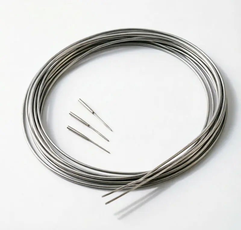
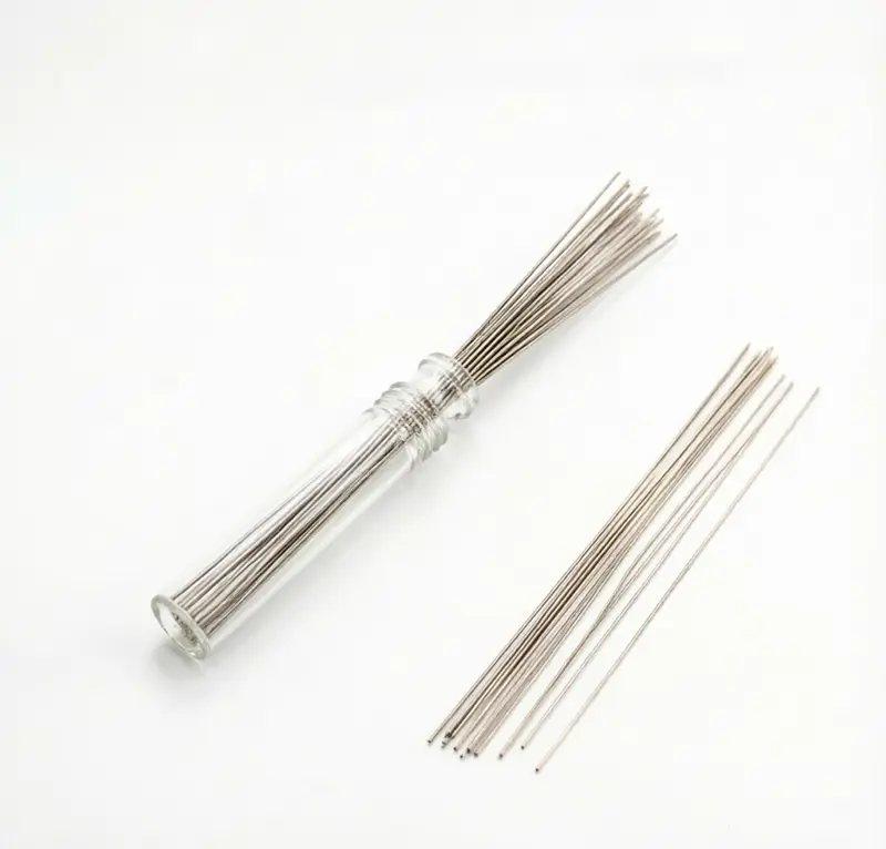
Palladium Alloy Wire
-
Product Description
Palladium alloy wire is a high-performance alloy material specifically designed for testing throughout the entire semiconductor lifecycle. It is widely used in wafer probing during the front-end of semiconductor manufacturing and in final product packaging testing during the back-end. Through a precise alloying process, this material achieves good mechanical hardness and fatigue resistance whilst ensuring good electrical conductivity. JFM’s palladium alloy wire solutions are designed to meet the stringent requirements for material performance stability in high-density, high-frequency testing environments, effectively balancing testing accuracy with consumable costs.
Key Features
Palladium-based alloy wires are suitable for precision test probe applications and offer the following characteristics:
- Stable low contact resistance
- High hardness and wear resistance
- Good machinability and formability
- Good fatigue resistance
- Balanced overall performance
Application Areas
Palladium-based alloy wires are primarily used in the following semiconductor testing and electronic inspection scenarios:
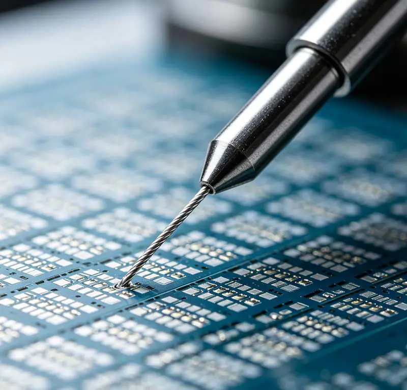
- Wafer testing probes: Used as the core wire material in cantilever probe cards.
- IC packaging testing: Used as conductive contacts for vertical probes and various high-density test sockets.
- Precision connector testing: Suitable for micro-test fixtures requiring precise contact force.
- High-frequency signal testing: Used in scenarios requiring signal integrity during the testing of communication chips and RF devices.
Product Specifications
| Parameter Category | Capabilities & Features |
| Material System | Using a palladium-based precious metal alloy system |
| Purity grades | Wire of various purity grades can be customised to meet specific requirements |
| Wire Diameter and Specification Range | A wide range of wire diameters and specifications are available to suit various probe types and fine-pitch structural design requirements |
| Compatible processes | Suitable for precision tip grinding, micro-welding, automated probe insertion and other probe processing techniques |
| Applications | Suitable for various probe manufacturing and testing scenarios, including semiconductor wafer testing and IC packaging testing |
* For further product information and application support, please contact us