What Are Conductive Ceramic Arms? An Analysis of Key Characteristics
-
2026-04-13 Industry News


Conductive ceramic arms are precision components combining conductivity, thermal stability, and mechanical strength. This article explains their key characteristics and industrial applications.
Introduction
In the field of wafer manufacturing, as performance requirements for semiconductor products continue to rise, semiconductor manufacturing processes and process technologies have also shown significant advancements. In advanced processes, wafer transfer systems impose increasingly stringent requirements on the material reliability and electrical conductivity of their end effectors (End Effector)/ceramic arms.Traditional metal arms often face challenges such as short service life, susceptibility to wear, susceptibility to electrostatic interference, and insufficient stability under special operating conditions such as high temperatures, corrosion, or the need for electrostatic protection. Conductive ceramic arms, leveraging their superior material properties and modern manufacturing processes, are gradually being applied in numerous leading process nodes of advanced semiconductor manufacturing, high-demand advanced laboratories, and complex industrial automation fields.
What is a Conductive Ceramic Arm?
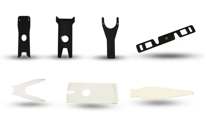
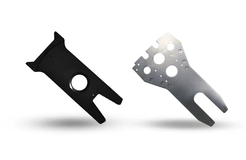
Also known as wafer handling arms, end-effectors, ceramic handling arms, or ceramic manipulators, the Conductive Ceramic Arm is a precision handling device featuring a high-performance conductive ceramic skeleton, specifically designed for the transfer and handling of wafers in semiconductor manufacturing.Through sintering, coating processes, and optimized joint design, this component achieves a balance of structural rigidity, anti-static control, and operational accuracy while ensuring high structural rigidity. It effectively meets the stringent requirements of advanced semiconductor processes for cleanliness, precision, and reliability.
Core Structural Components:
• Ceramic Skeleton: High hardness, high rigidity, low thermal expansion coefficient
• Conductive layer/grid: Discharges static electricity to protect electronic components
• High-precision joint system: Supports micron-level repeatable positioning
• Surface anti-corrosion coating (optional): Enhances resistance to acids and alkalis
Advantages of the Conductive Ceramic Arm
High-Temperature Stability
Ceramic materials inherently possess excellent high-temperature resistance, maintaining structural and motion precision stability even in prolonged high-temperature environments. In advanced semiconductor processes, wafers may undergo heat treatment, deposition, or etching. Conductive ceramic arms can reliably handle wafers in high-temperature environments, preventing minute displacements caused by thermal deformation and thereby ensuring wafer precision and yield.
Anti-static and Conductive Properties
Conductive ceramic arms achieve uniform surface conductivity through specialized processes, providing excellent static discharge capabilities. In advanced semiconductor processes, reaction residues and charged particles easily accumulate on wafer surfaces, posing risks of electrostatic attraction or discharge. If not handled properly during handling, this can easily cause damage to the wafers.Conductive ceramic arms can rapidly dissipate residual charges, reducing the defect rate caused by static electricity and thereby improving manufacturing stability and overall yield.
Wear and Corrosion Resistance
Ceramic materials possess high hardness and, through surface optimization, exhibit excellent wear resistance and chemical corrosion resistance. During wafer transfer, photomask handling, or cleaning processes, the arm must operate for extended periods in chemical solutions or high-friction environments. The conductive ceramic arm maintains precise handling and stable performance under these harsh conditions, extending equipment lifespan and reducing maintenance costs.
Lightweight Design and High Responsiveness
Compared to traditional metal arms, ceramic arms are lighter in weight, reducing drive loads and thereby increasing motion speed and operational sensitivity. In high-frequency operation scenarios such as semiconductor wafer handling, the lightweight design enables the arm to respond promptly to commands, minimizing potential damage to wafers caused by vibration or swaying, and consequently improving overall production efficiency.
High-Precision Manipulation Capabilities
Combining high-rigidity ceramic materials with precision joint design, conductive ceramic arms support highly repeatable positioning and fine motion control. In advanced wafer handling, optical component manipulation, or demanding experimental applications, conductive ceramic arms deliver precise handling and stable operation even under complex conditions and in the presence of minute residual charges, ensuring wafer quality and equipment reliability.
Ceramic Arms vs. Metal Arms
|
VS |
Conductive Ceramic Arm |
Metal Arm |
|
High-temperature resistance |
High, long-term stability |
Prone to thermal expansion and deformation |
|
Anti-static |
Built-in conductive layer, stable and relialie |
Requires external grounding; complex operation |
|
Corrosion-resistant |
Resistant to acidic and alkaline solvents |
Prone to corrosion; requires coating protection |
|
Accuracy |
Micron-level |
Accuracy is affected by heat and wear |
|
Weight |
Lightweight |
Heavy, high power consumption |
Conclusion: In environments requiring high precision, high-temperature resistance, anti-static properties, or resistance to high corrosion, conductive ceramic arms offer significant advantages, making them a widely adopted material solution in advanced semiconductor processes and industrial automation.
Common Industry Applications
|
Scenarios |
Technical Requirements |
Advantages of Ceramic Arms |
|
Semiconductor Production Lines |
Anti-static, high-temperature handling |
Rapid static discharge, high-temperature resistance, and high stability |
|
Optical Component Assembly |
Micron-level repeatability |
High hardness, low thermal expansion |
|
Chemical laboratories |
Resistant to acids, alkalis, and high temperatures |
Corrosion-resistant, heat-resistant, long-term reliability |
|
Automated production lines |
High-frequency operation, lightweight |
High rigidity, high sensitivity |
|
Vacuum conveying systems |
Precision handling in vacuum environments, anti-static |
High electrical conductivity, vacuum resistance, precise control of minute displacements |
|
Atmospheric transfer system |
High-frequency wafer handling, residual charge control |
Rapid static dissipation, wear and corrosion resistance, stable operation |
Conductive ceramic arms play a critical role in semiconductor wafer handling and advanced manufacturing processes. They enable fast and stable wafer handling, minimizing the impact on wafer quality caused by static charge buildup or residual reactants, thereby improving yield and production efficiency.At the same time, their high wear resistance, high conductivity, and high precision reduce equipment downtime and maintenance costs, ensuring the stable operation of the entire process and providing reliable process assurance and sustained value for semiconductor manufacturing.
Conductive Ceramic Arm Selection Guide
• Temperature Resistance: Select the appropriate high-temperature rating based on the operating environment
• Electrical Conductivity: In electrostatic-sensitive environments, prioritize arms with controllable surface resistivity
• Precision and Rigidity: Micron-level operations require a highly rigid frame and high-precision joints
• Corrosion Resistance: Select surface coating types that match process requirements
• Weight and Joint Design: Support high-frequency, sensitive operations
Conclusion
With their comprehensive advantages—including high-temperature resistance, anti-static properties, wear resistance, lightweight design, and high precision—conductive ceramic arms are suitable for applications in semiconductors, industrial automation, electronics manufacturing, and scientific research. When selecting a model, companies should consider the application environment, precision requirements, and material characteristics to ensure optimal production efficiency and equipment stability.
If you would like to learn more about the technical specifications or customization options for conductive ceramic arms, please contact JFM. We will provide you with detailed selection guidance and technical support!


