High Precision Wafer Handling Arm for Chip Production
-
2026-04-13 Industry News


High-precision wafer handling arms are critical components in semiconductor manufacturing, designed to ensure stable, contamination-free wafer transfer with exceptional accuracy, rigidity, and thermal stability in cleanroom environments.
Introduction
In the semiconductor manufacturing industry, wafer handling precision is one of the key factors affecting production yield and chip performance. As wafer sizes have gradually transitioned from 200 mm to 300 mm and beyond, wafer weight has increased, their structure has become thinner and more fragile, and the complexity of manufacturing processes has significantly risen.Minor deviations during handling may lead to surface scratches, particle contamination, or potential wafer loss, posing a severe challenge to the stability of advanced processes and product reliability.
A s a core transfer device in modern semiconductor production lines, the wafer handling arm serves a purpose far beyond simply transferring and positioning wafers.They are directly involved in high-precision collaborative operations within ultra-clean environments, requiring nanometer-level positioning accuracy, low vibration, and minimal particle contamination, while also balancing high-speed operation with stability and even possessing certain electrical conductivity. Wafer handling technology has become a critical factor in enhancing overall line capacity, reducing unit manufacturing costs, and supporting process consistency.
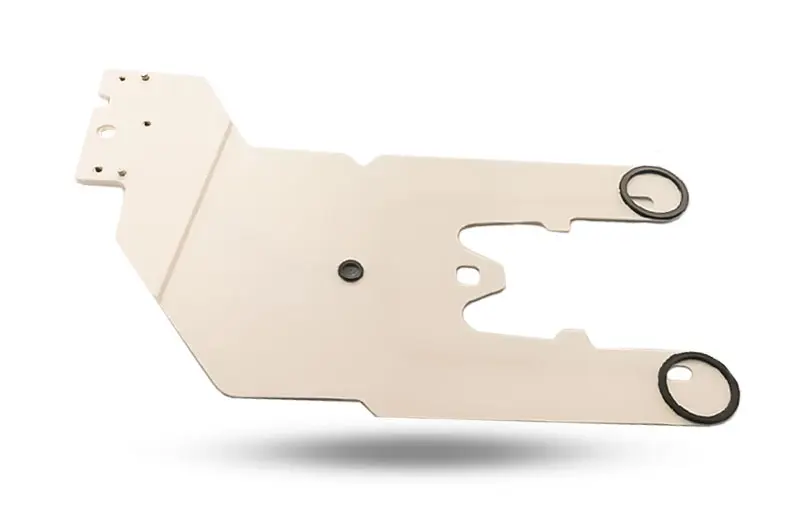
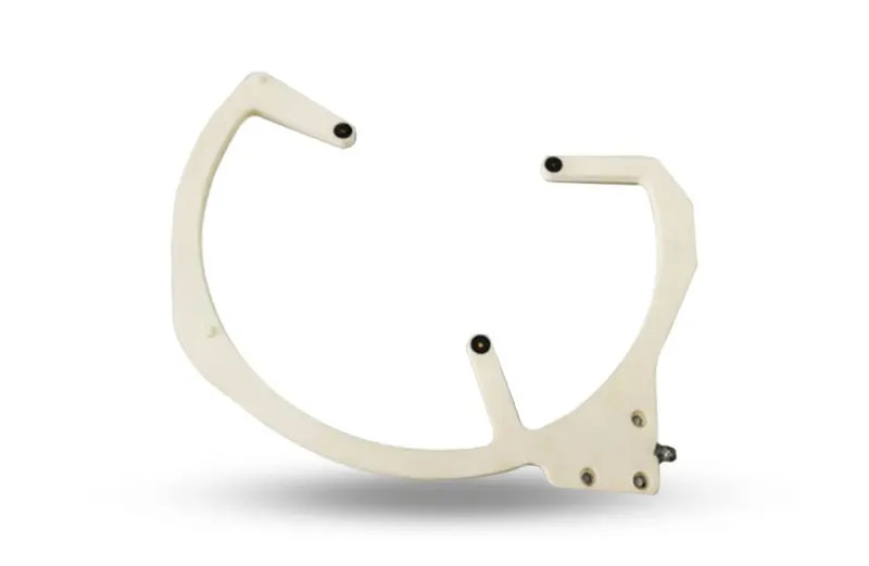
What Is a Wafer Handling Arm
A wafer transfer arm is a high-precision automated handling device used in semiconductor equipment. It is primarily designed to transfer wafers stably and accurately between different process steps while ensuring their surfaces remain free of scratches and contamination. Its design features include:
1. Non-contact or low-contact handling technology
Utilizing technologies such as vacuum suction, electrostatic gripping, flexible end-effectors, or air-bearing support to minimize physical contact with the wafer and prevent damage to sensitive areas.
Equipped with adaptive control capabilities, it automatically adjusts suction force or gripping pressure based on the wafer’s thickness and material properties to maintain stable and reliable handling.
2. Anti-contamination and anti-static design
Utilizes anti-static aluminum alloy, carbon fiber, or special engineering composite materials, with key contact areas coated with anti-static coatings to prevent particle adhesion caused by static electricity buildup.
Sealed structural design is adopted to help reduce the generation and accumulation of fine dust, maintaining cleanliness during wafer handling.
3. High-Precision Positioning and Dynamic Control
Equipped with built-in laser sensors, vision recognition systems, and encoders to support micron-level positioning accuracy and dynamic posture correction.
Real-time adjustment of wafer angle and height is supported to meet the stringent positioning accuracy requirements of processes such as lithography, etching, and thin-film deposition.
4. Automation and Production Line Integration
Compatible with standard FOUPs (Front Opening Unified Pods), material handling systems, and various semiconductor equipment interfaces to enable fully automated handling on the production line.
It can work in conjunction with MES (Manufacturing Execution System) to optimize production cycles, track materials, and enable intelligent scheduling, thereby enhancing overall production line efficiency and operational flexibility.
 |
 |
The Key Role of Wafer Handling Arms
1. Improving Production Yield
During wafer handling, positioning errors or improper operation can easily cause scratches on the wafer surface, particle contamination, or even breakage. High-precision handling arms, through stable and low-contact handling methods, can reduce wafer loss to a certain extent, playing an important role in ensuring wafer integrity and cleanliness.
2. Improving Production Efficiency and Throughput
Automated wafer handling arms enable continuous, high-speed wafer transfer and support synchronized handling operations across multiple process equipment stations.
3. Supporting process consistency and Quality Control
With sub-micron positioning capabilities and real-time posture adjustment functions, the handling arm helps ensure that wafers remain in their intended positions during critical processes such as lithography, etching, and thin-film deposition. This effectively reduces process fluctuations caused by placement deviations, thereby ensuring consistent chip performance and overall quality.
4. Reducing Operating Costs and Production Risks
By reducing manual intervention and wafer breakage, the wafer handling arm helps lower the overall operating costs of the production line. It also minimizes the risk of wafer scrap and equipment downtime caused by improper operation, thereby enhancing production reliability.
Typical Semiconductor Applications
1. Lithography Process
In the lithography process, wafers require high-precision alignment and positioning to ensure critical dimensions and overlay accuracy. Through micron-level positioning and real-time posture control, the handling arm helps reduce wafer deformation and micro-scratches, helping to lower lithography defect rates and enhance process stability.
2. Etching and Deposition Processes
In processes such as dry etching, CVD, and PVD, wafers are particularly sensitive to particle contamination and static electricity buildup. The handling arm features a cleanroom-grade design and anti-static materials to reduce particle adhesion and surface damage during transport, thereby optimizing process uniformity and reducing wafer scrap rates.
3. Testing and Packaging Processes
During wafer electrical testing and subsequent packaging, the handling arm enables efficient wafer transfer between different modules, supporting continuous automated production. This increases overall throughput, reduces manual intervention, and enhances the production line’s overall operational efficiency and equipment utilization.
4. Multi-Size Wafers and Special Materials
When handling silicon wafers of various sizes as well as compound semiconductor materials such as GaN and SiC, the handling arm features adaptive gripping force and flexible end-effector configuration capabilities. This ensures compliance with diverse material properties and process requirements, maintaining high reliability and transfer precision even during specialized processes.
Conclusion
Wafer handling arms are not only critical transfer components in semiconductor manufacturing lines but also important technological equipment for supporting process yield, increasing production capacity, and achieving process optimization. Selecting high-precision, high-reliability wafer handling arms has become a vital component for modern semiconductor companies to strengthen their competitiveness.
JFM is committed to providing customers with a variety of mechanical handling arm solutions, covering multiple process scenarios from lithography and etching to thin-film deposition and packaging and testing. We help customers achieve high-precision wafer positioning, clean transfer, and automated scheduling, helping optimize overall line capacity and product yield. Contact us today for customized technical support and solutions.
Wafer Handling Arm FAQ
Q1: How compatible are wafer handling arms with different semiconductor processes?
A1: Modern high-performance wafer handling arms typically offer strong process compatibility and can be used in critical processes such as lithography, etching, thin-film deposition, and test and packaging. Some models are equipped with self-adjusting suction force or flexible gripping units, enabling them to adapt to wafers of different materials, thicknesses, and surface conditions, thereby meeting the specific requirements of various semiconductor processes.
Q2: How do wafer handling arms prevent electrostatic discharge (ESD) and particle contamination in cleanroom environments?
A2: Manipulators commonly utilize anti-static materials, anti-particle coatings, and enclosed or semi-enclosed mechanical structures to effectively control static buildup and particle release. Additionally, vacuum suction systems are typically integrated with high-performance filtration units to further maintain a clean environment during wafer handling.
Q3: Does the speed of the wafer handling arm affect processing accuracy?
A3: High-speed operation may introduce micro-vibrations and positioning deviations, adversely affecting wafer positioning during high-precision processes such as lithography and inspection. To address this, wafer handling arms are typically equipped with high-response servo control systems and motion planning algorithms. By optimizing motion trajectories and acceleration/deceleration strategies, they maintain stable positioning accuracy at the micrometer level while ensuring transfer efficiency.
Q4: What are the common materials and surface treatment processes used for wafer handling arms?
A5: Common materials include aluminum alloys, carbon fiber-reinforced composites, or specialty engineering plastics, which strike a balance between high rigidity and lightweight design. Surfaces are typically treated with anodizing, Teflon, or diamond-like carbon (DLC) coatings to enhance wear resistance and anti-adhesion properties, while reducing particle generation and electrostatic attraction. These materials contribute to lightweight construction and excellent durability.
Q5: How should one select the appropriate wafer handling arm for a semiconductor production line?
A5: Selection requires a comprehensive evaluation of wafer size specifications, precision and cleanliness requirements for process steps, equipment automation integration capabilities, and compatibility with production line cycle times. Generally, high-reliability models with high positioning accuracy, strict contamination control, and support for communication with MES systems and equipment should be prioritized to meet the demands of modern semiconductor manufacturing for efficient, stable, and intelligent handling.


