Understanding Leadless Ceramic Packages: Structures and Uses
-
2026-04-17 Industry News


Understand leadless ceramic package structures and their practical uses. A concise guide to help engineers choose reliable solutions for high-performance electronic applications.
Introduction
As electronic packaging continues to evolve toward higher density and miniaturization, leadless ceramic packages have gradually emerged as a structural form worthy of attention. Unlike traditional leaded packages, this type of package achieves electrical connections through bottom pads or contact surfaces, demonstrating certain advantages in terms of space utilization, structural compactness, and high-frequency performance compatibility.
What Is a Leadless Ceramic Package
A leadless ceramic package refers to a structure that uses ceramic material as the packaging substrate and does not employ exposed metal leads; instead, it connects to the circuit board via metallized pads or contact areas on the bottom of the package.
Its typical features include:
• No external lead structure
• Connection via metallized pads on the bottom or edges
• Relatively compact overall structure
• Often combined with hermetic packaging processes (depending on the design)
In terms of signal routing, signals are transmitted directly via internal conductors to the bottom soldering area, reducing the path length associated with traditional leads. This is particularly significant in certain high-frequency or high-speed applications.
Core Structure of Leadless Ceramic Packages
Understanding pinless ceramic package hinges on the design of its internal and external connection methods.
1. Ceramic Substrate
Common materials include aluminum oxide (Al₂O₃) and aluminum nitride (AlN). Different materials vary in thermal conductivity and electrical insulation properties; the specific choice is typically evaluated based on application requirements.
2. Chip Mounting
The chip is secured to the ceramic substrate using thermal adhesive or solder. This step influences the thermal conduction path and the overall structural stability.
3. Gold Wire Bonding
Gold or aluminum wires are used to connect the chip to the internal circuitry, serving as a critical component for signal transmission within the package.
4. Metalized Pads
The metallized area on the bottom of the package is used for soldering to the PCB and is a key feature that distinguishes it from leaded structures.
5. Package Type
Depending on design requirements, either an open-air structure or an airtight packaging structure can be adopted to accommodate different environmental conditions.
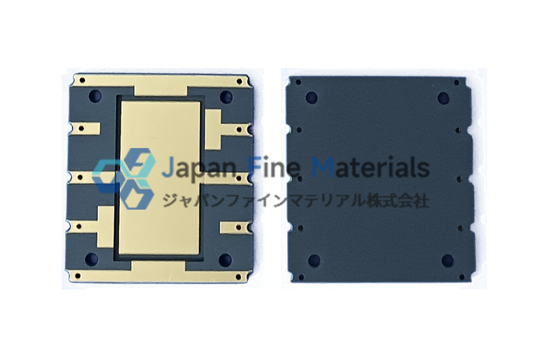
Leadless Ceramic Package Types
In practical product applications, leadless ceramic packages primarily refer to structures without exposed metal leads, where connections are achieved via bottom pads or contact arrays.
Ceramic Leadless Chip Carrier (CLCC)
CLCC is one of the typical leadless ceramic package forms. The pads are usually distributed along the bottom edge of the package, offering a balance between connection stability and compact layout.
Structural Features:
• No exposed leads, reducing the complexity of the package profile
• Peripheral pad design facilitates alignment with PCB pads
• The ceramic substrate offers excellent electrical insulation properties
• Can be combined with hermetic packaging processes, making it suitable for environmentally sensitive applications
Applications:
• Industrial electronic modules
• Communication circuits
• Miniaturized functional components
CLCC is better suited for applications that have certain requirements for package size and long-term operational stability, but do not require high pin density.
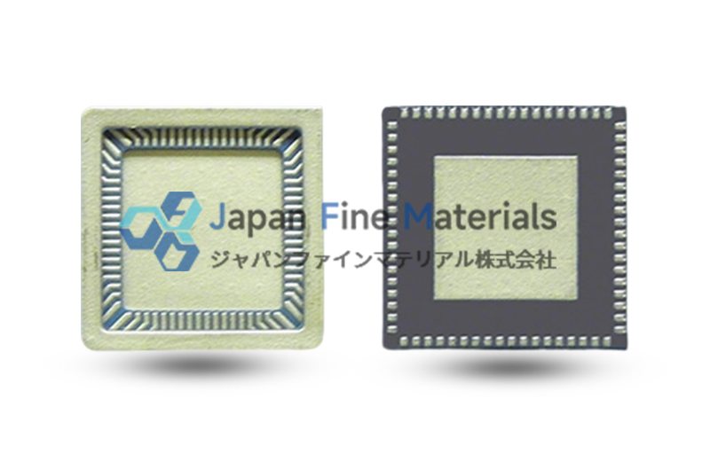
Ceramic Quad Flat No-Lead Package (CQFN)
CQFN features a multi-pad layout on the bottom and can incorporate a central heat dissipation area, making it widely used in today’s highly integrated designs.
Structural Features:
• Bottom multi-pad design enhances connection density
• Central heat sink pad helps optimize thermal conduction paths
• Low package height facilitates compact layouts
• Relatively simplified signal paths, suitable for certain high-frequency applications
Applications:
• Power management circuits
• High-frequency signal processing modules
• Compact PCB design scenarios
CQFNs typically require coordinated optimization with PCB thermal structures (such as via arrays) to achieve more effective thermal management.
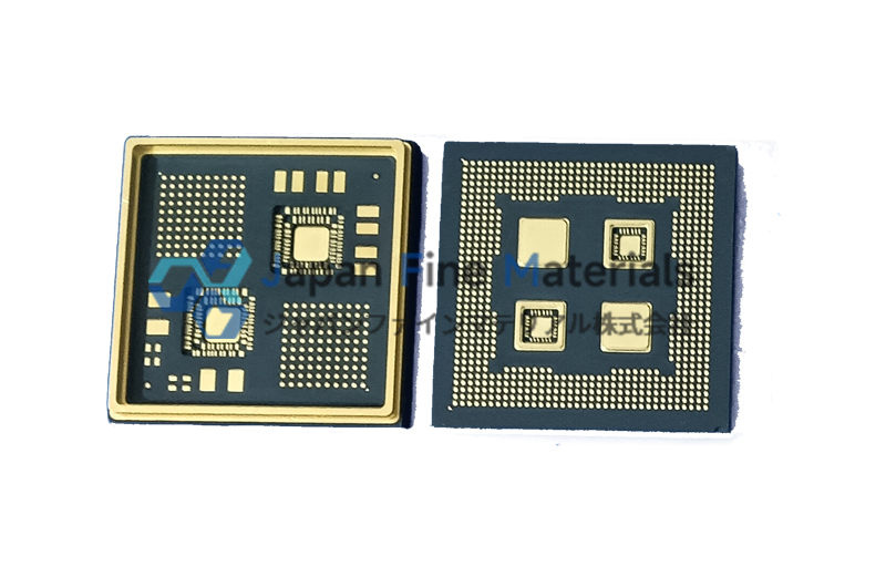
Ceramic Land Grid Array (CLGA)
CLGA achieves connectivity through a bottom-side array of pads and is a leadless package designed for applications requiring a high pin count and high integration.
Structural Features:
• Pads are arranged in a grid array, supporting higher I/O density
• The leadless structure helps shorten signal paths
• Package dimensions can be adjusted within a certain range as needed
• Suitable for multilayer ceramic structure designs
Applications:
• Multi-channel signal systems
• High-density integrated circuits
• Electronic modules with complex functionality
CLGA is better suited for designs with specific requirements regarding pin count and space utilization, and requires coordination with soldering and inspection processes during the PCB design phase.
Pinless and Pinned Ceramic Packages
During the package selection process, leadless and leaded structures are often evaluated simultaneously. The main differences are as follows:
|
VS |
Leadless ceramic packages |
Leaded Ceramic Packages |
|
Connection Method |
Bottom pads |
External metal leads |
|
Package Volume |
More compact |
Relatively large |
|
Assembly method |
SMT mounting |
Through-hole or surface mount |
|
Stress distribution |
Concentrated in the solder joint area |
Leads can act as buffers |
From an engineering perspective, each type of package is suited to different design constraints, and there is no single standard answer.
Typical Applications
Leadless ceramic packages are commonly found in electronic systems with specific requirements for spatial layout, signal routing, and package consistency. Compared to traditional leaded structures, these packages align more easily with modern electronic design philosophies in terms of board-level integration and structural compactness.
1. Communication Equipment
In high-frequency or high-speed signal applications, the package structure is highly sensitive to signal path length and connection methods. Leadless designs reduce the path extension caused by external leads, making the overall connection more direct. In scenarios such as RF modules and small communication units, this structure is more compatible with high-density PCB designs.
2. Industrial Electronics
In industrial control or automation equipment, circuit systems often need to balance size constraints with long-term operational requirements. Leadless ceramic packages are not only structurally compact but also facilitate layout on multilayer PCBs, helping to improve space utilization. In operating conditions with significant temperature fluctuations or extended runtime, a well-designed package structure helps maintain overall stability.
3. Power and Control Modules
As power modules evolve toward higher power density, packaging must not only provide electrical connectivity but also support thermal management design. Certain leadless packages (such as those with a central pad structure) can serve as part of the thermal conduction path in the design, working in conjunction with the PCB’s heat dissipation structure to achieve more efficient heat distribution within a compact space.
4. Miniaturized Electronic Systems
In electronic devices with strict size constraints, leadless ceramic packages reduce the space occupied by peripheral structures, resulting in a more compact overall design. Such packages facilitate standardized layouts in highly integrated modules and are well-suited for automated placement processes.
Design and Selection
As an important form within the electronic packaging system, leadless ceramic packages offer greater possibilities in terms of structural compactness and design adaptability.
In practical projects, when selecting leadless ceramic packages, the following factors should typically be considered comprehensively:
Pad Design and PCB Compatibility
The size, spacing, and layout of the pads directly impact assembly quality and subsequent performance.
Thermal Management Pathways
Whether to include a central heat sink pad and how it integrates with the PCB’s thermal management structure are key design considerations.
Material Selection
Different ceramic materials vary in terms of thermal conductivity and mechanical properties; they should be evaluated based on actual operating conditions.
Process Adaptation
This includes mounting processes and reflow soldering parameters, which must be compatible with the packaging structure.
If you are evaluating how different ceramic package structures can be adapted for your project, or if you need to select packaging options and optimize structures based on specific applications, you can learn more about various leadless ceramic packages and related product solutions.
JFM offers a variety of ceramic packaging options to help achieve a more suitable balance between structural design and application requirements.


