How Ceramic Insulation Rings Enhance Semiconductor Reliability
-
2026-04-14 Industry News


Ceramic insulation rings enhance reliability in semiconductor equipment by providing excellent electrical insulation, thermal resistance, and dimensional stability under extreme processing conditions.
Electrical Risks and Challenges in Semiconductor Manufacturing
Semiconductor manufacturing is a highly complex and precision-demanding field in today’s industrial landscape. As advanced processes continue to advance toward 5nm, 3nm, and even 2nm nodes, wafer processing equipment must maintain long-term stable operation in high-voltage, high-frequency, and high-energy plasma environments.Whether it is plasma etching, chemical vapor deposition (CVD), or ion implantation, these critical processes involve high-electric-field environments and are accompanied by harsh operating conditions such as high temperatures and highly corrosive reaction gases.
Under such complex physical and chemical loads—including electrical and gaseous stresses—insulation failure, electrical leakage, or dielectric breakdown can lead to unexpected equipment shutdowns, process parameter drift, and reduced wafer yield. Therefore, ensuring the electrical insulation reliability of high-voltage components has become a critical challenge in safeguarding the overall performance and mass production stability of semiconductor equipment.As a key component capable of withstanding high voltage and resisting plasma erosion, the ceramic insulation ring plays a crucial role in this process.
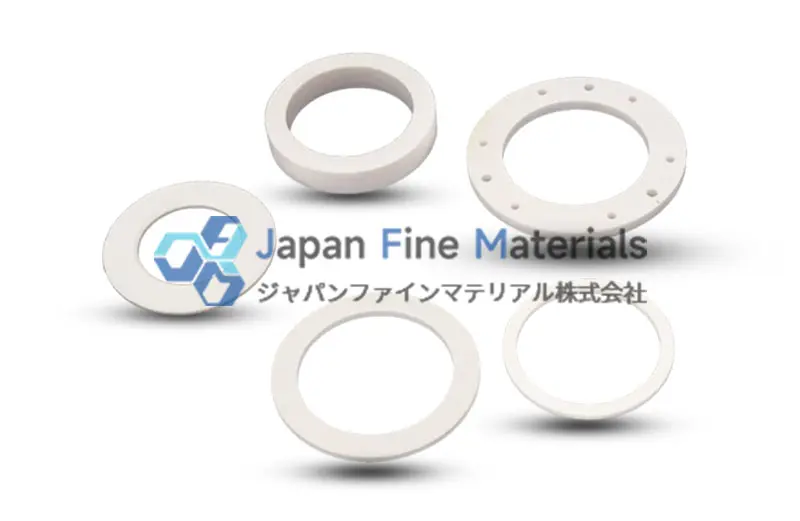
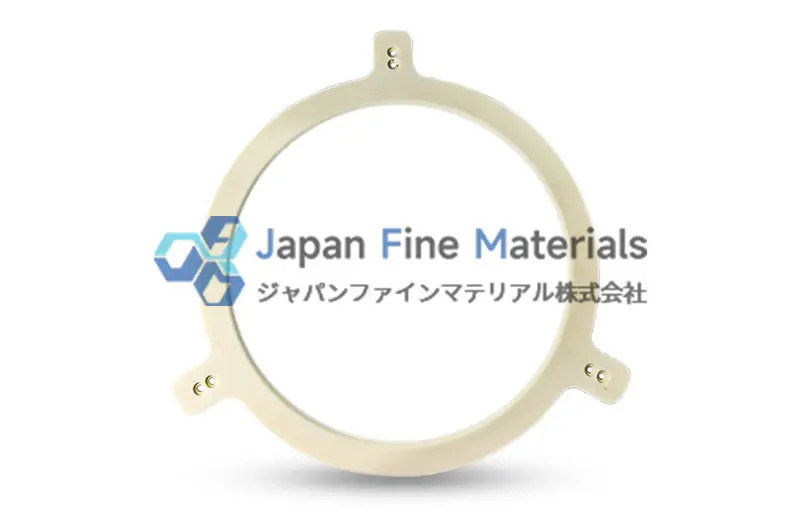
What is a Ceramic Insulation Ring?
A ceramic insulation ring is a critical electrical isolation component in semiconductor manufacturing equipment, typically installed between the electrode and the reaction chamber to provide insulation in high-voltage environments. It not only effectively prevents high-voltage breakdown or arc discharge between the electrode and the chamber but also optimizes the electric field distribution in the process area, enhances plasma uniformity, and ensures etching or deposition accuracy during wafer processing.
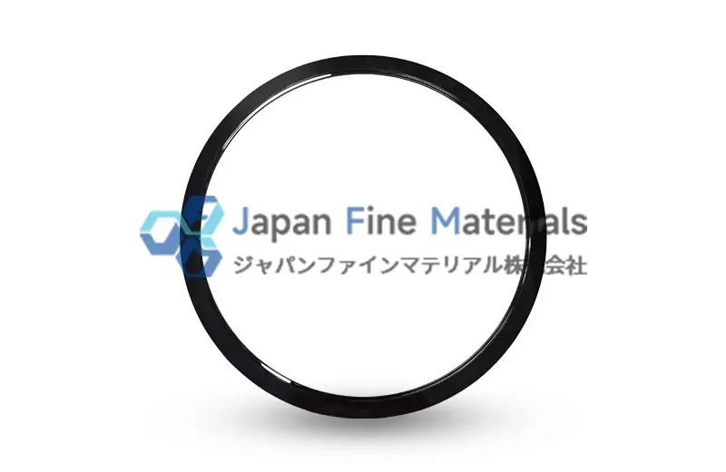
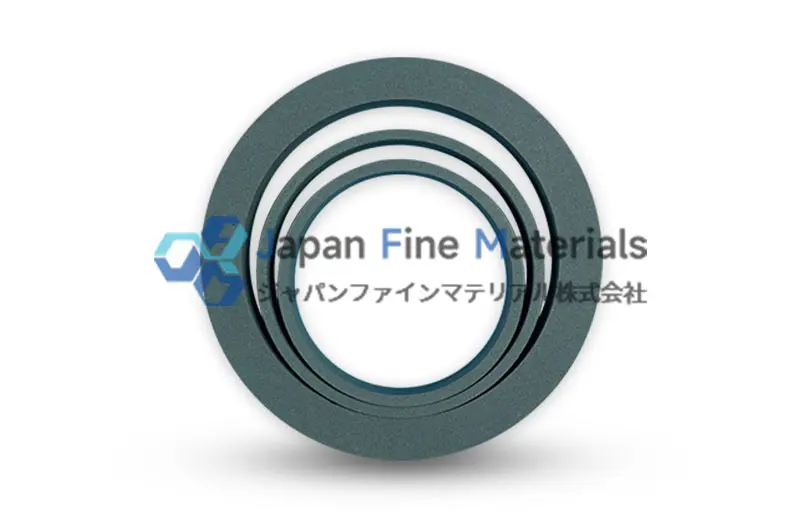
In terms of material selection, ceramic insulation rings must balance high dielectric strength, excellent thermal stability, and resistance to plasma erosion. Currently, the commonly used materials include the following categories:
• Aluminum oxide (Al₂O₃): Offers excellent overall performance, high dielectric strength, stable mechanical properties, and moderate cost; commonly used in medium- and low-power process equipment.
• Yttrium oxide (Y₂O₃): Possesses excellent resistance to plasma corrosion and high toughness, making it suitable for high-frequency, high-power reaction chambers, particularly in environments with corrosive gases.
• Aluminum nitride (AlN): In addition to good electrical insulation, it possesses a high thermal conductivity, effectively dissipating heat generated during the process, making it suitable for applications with high heat dissipation requirements.
• Silicon Carbide (SiC): With high hardness, wear resistance, and excellent overall performance, it is commonly used in environments with high mechanical and thermal loads, such as high-energy ion implantation.
• Porous Ceramic: With controllable gas permeability and lightweight properties, it is suitable for special process requirements, such as uniform atmosphere distribution or back-blow gas structure design.
 |
 |
 |
Electrical Safety Functions of Ceramic Insulation Rings
1. High-Voltage Insulation and Protection Against Dielectric Breakdown
In advanced plasma processes (such as ICP etching and PECVD), high voltages of several thousand volts are often applied to RF or DC electrodes. If the insulation between the electrodes and the grounded chamber is insufficient, it may cause dielectric breakdown or arc discharge, which can damage the electrodes and even result in the scrapping of an entire wafer due to chamber contamination.With superior dielectric strength, ceramic insulating rings provide a robust insulation barrier for the core process area, helping to prevent high-voltage breakdown and improving the reliable operation of the equipment.
2. Optimizing Electric Field Distribution to Ensure Process Uniformity
In integrated circuit manufacturing, plasma uniformity directly determines line width consistency and yield on the wafer.The dielectric properties and three-dimensional structure of ceramic insulating rings are key factors in regulating the electric field distribution within the reaction chamber. By optimizing the shape and material of the insulating ring (such as a specific dielectric constant), it is possible to mitigate edge effects in the electric field, preventing excessive etching or abnormal deposition rates at the wafer edges. This ensures process uniformity across the entire wafer, meeting the stringent requirements of advanced processes for process windows.
3. Controlling Current Leakage and Reducing Energy Consumption
In complex plasma chemical environments, low-quality insulating materials are prone to continuous micro-current leakage. Such leakage not only increases energy waste but also disrupts impedance matching and potential distribution within the chamber, causing process parameter drift and thereby affecting the control accuracy of feature dimensions (CD).High-purity ceramic materials possess excellent volume resistivity, effectively blocking leakage pathways. This not only reduces auxiliary energy consumption but also ensures the long-term stability of plasma conditions, providing a solid foundation for mass production consistency.
The Value of Insulation Rings to Process and Production Capacity
1. Ensuring Process Stability and Consistency
High-performance ceramic insulating rings provide stable and reliable electrical isolation in high-voltage, high-frequency, and intense plasma environments. They effectively suppress arc breakdown and microcurrent leakage, ensuring that critical process parameters—such as etch rates and deposition thickness—remain highly consistent during prolonged operation, effectively reducing batch-to-batch variation.
2. Supporting Continuous Equipment Operation and Production Output
With superior high-temperature resistance, plasma corrosion resistance, and extended service life, ceramic insulating rings help extend the continuous operation cycle of equipment, reducing unplanned downtime and maintenance frequency. This effectively improves overall equipment utilization and supports wafer production lines in achieving higher throughput.
3. Ensuring Wafer Yield and Product Consistency
Stable insulation properties ensure uniform plasma distribution, thereby reducing process issues such as etch residue and film thickness non-uniformity at the source. This helps improve wafer surface uniformity and reduce scrap rates, which in turn has a positive impact on overall yield and process stability.
4. Optimizing Total Operating Costs
Although the initial procurement cost of high-performance ceramic insulating rings is relatively high, their positive impact on equipment reliability, reduced maintenance frequency, and product yield effectively lowers the manufacturing cost per wafer, thereby achieving a more advantageous cost structure at the overall operational level.
Conclusion
As a critical component in semiconductor manufacturing equipment, the ceramic insulating ring, despite its compact structure, plays a critical role in ensuring process stability and reliable equipment operation. Through effective electrical insulation, uniform electric field control, and superior energy consumption management, it not only enhances equipment operational stability but also directly impacts wafer processing yield and production efficiency.
As semiconductor manufacturing advances toward more advanced processes such as 3nm and 2nm, higher demands are placed on the insulation rings’ voltage withstand capability, resistance to plasma erosion, and long-term reliability. Against this backdrop, the technical value of high-performance ceramic insulation rings is becoming increasingly prominent, serving as a vital foundation for the continuous optimization of advanced process equipment.
If your project requires insulation solutions for high-power, highly corrosive process environments, JFM can provide high-performance ceramic insulator ring solutions. We support material selection and structural customization to help you achieve stable equipment operation and optimized process performance. Please contact the JFM team for tailored product support and technical consultation.
FAQ
Q1: What is the maximum voltage that an insulating ring can withstand in semiconductor equipment?
A1: Insulation rings are made of high-performance ceramic materials with excellent dielectric properties. They can withstand the high-voltage RF environments common in advanced processes, effectively preventing arc breakdown or dielectric breakdown between electrodes and chambers, and ensuring the stable operation of plasma processes.
Q2: Why choose ceramic over plastic or quartz?
A2: Compared to plastic or quartz, ceramic materials demonstrate superior performance in terms of high-temperature resistance, resistance to plasma erosion, and mechanical stability. They are well-suited for high-power, highly corrosive process chambers, helping to ensure the uniformity of wafer processing and the reliability of equipment operation.
Q3: How often do the insulating rings need to be replaced?
A3: The service life of an insulating ring is influenced by various factors, including specific process conditions, power load, and material properties. In standard plasma environments, high-performance ceramic insulating rings typically have a long service life, significantly reducing equipment maintenance frequency and supporting continuous, stable production on the production line.
Q4: Can insulating rings be customized?
A4: Yes. We offer customized solutions tailored to customers’ equipment configurations, process types, and performance requirements, including dimensions, material selection, and insulation structures, to meet electrical insulation and process optimization needs across different process nodes.


