Ceramic Edge Rings in Etching and Deposition Processes
-
2026-04-14 Industry News


Ceramic edge rings play a critical role in etching and deposition equipment, helping stabilize plasma distribution and improve wafer process consistency in semiconductor manufacturing.
Introduction
Semiconductor manufacturing demands high levels of microscopic precision and process consistency, with etching and deposition being critical process steps that determine device performance and yield. Due to the difficulty in controlling process uniformity, the wafer edge region often exhibits defects, film thickness non-uniformity, and particle contamination. As a critical area affecting overall process stability, it requires effective optimization of the electric field distribution, reaction gas flow, and material deposition/removal behavior to effectively optimize process uniformity in this area, thereby ensuring process stability and product yield. The ceramic edge ring is one of the key process components influencing this process and recommended attention and quality assurance.
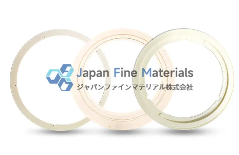
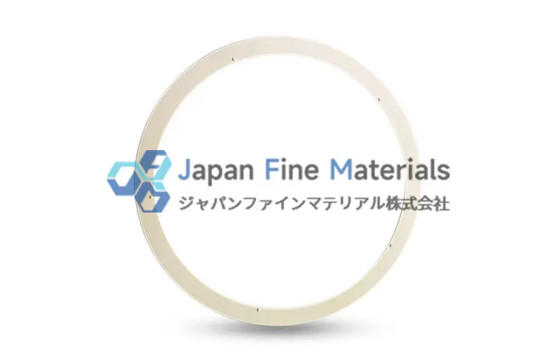
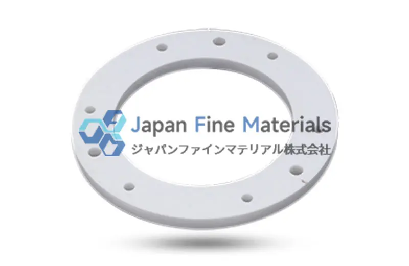
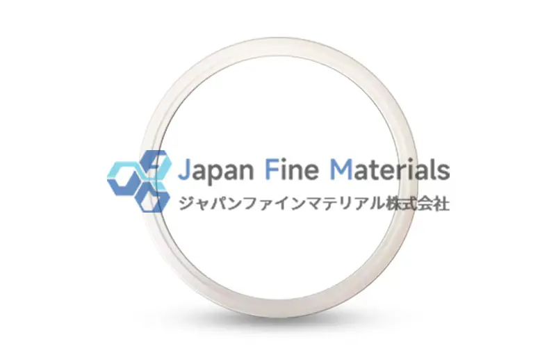
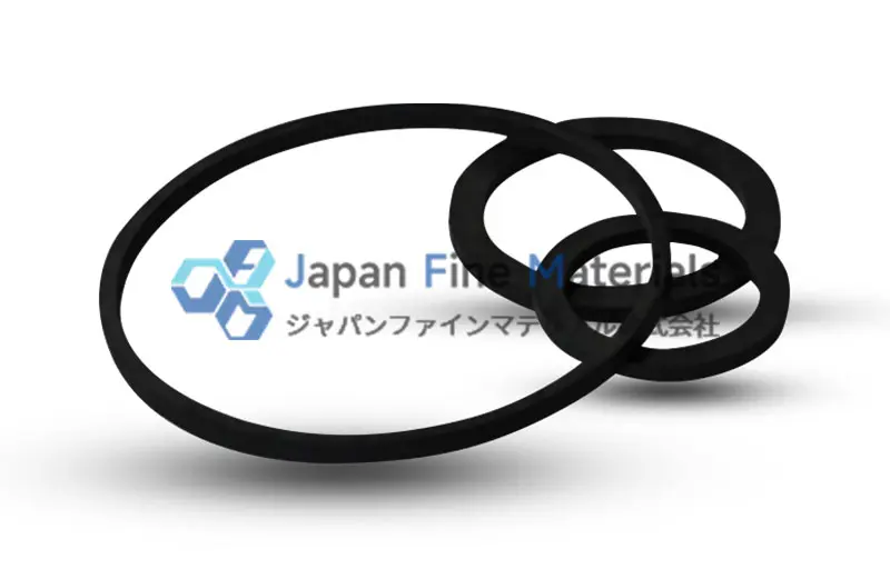
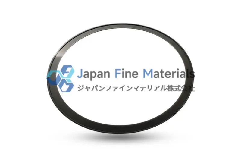
What is a Ceramic Edge Ring?
A Ceramic Edge Ring is a ring-shaped functional component installed inside the chamber of semiconductor thin-film deposition equipment or etchers, positioned in close contact with the outer edge of the wafer. It is primarily used to optimize the process uniformity of wafer etching. This component features corrosion resistance, excellent sealing properties, resistance to high and low temperatures, and high machining precision. Although it does not directly participate in the formation of circuit patterns, it serves as a important auxiliary element, playing a protective and optimizing role during the process.
Structurally, the Ceramics Edge Ring is typically ring-shaped, with an inner diameter precisely matched to the wafer’s diameter and an outer diameter that forms a stable fit with the chamber tray or electrodes. The ring’s thickness and geometric profile are rigorously designed to provide reliable mechanical support while effectively regulating gas flow and plasma distribution during the process.
Functionally, ceramic edge rings primarily serve the following purposes:
• Physical Isolation: Establishes an annular barrier between the wafer and the chamber environment, effectively blocking unnecessary physical or chemical interference from the outside.
• Edge Stability: The wafer edge is a high-risk area for defects (such as edge over-etching and film delamination); the ceramic edge ring helps mitigate such process anomalies.
• Particle Suppression: By covering the exposed areas of the wafer edge, it reduces particle shedding and contamination caused by irregular edge topography or microcracks.
• Chamber Protection: In certain processes, direct contact between plasma or reactants and the chamber walls can lead to deposition or corrosion issues. The ceramic edge ring serves as the first line of defense, reducing equipment contamination and wear.
In summary, ceramic edge rings are not merely mounting components but critical elements for ensuring process environment stability and yield rates. Their performance and condition directly determine whether semiconductor manufacturing processes can operate stably under high-precision and high-cleanliness requirements.
Role in Etching Processes
In dry etching or Deep Reactive Ion Etching (DRIE) processes, issues such as over-etching, uneven etch depth, or poor sidewall profiles often occur in the wafer edge regions. Ceramic edge rings optimize the behavior of plasma and reactive species at the wafer edges by adjusting the electric field distribution, ion incidence angle, and gas flow conditions in the edge region, thereby improving etch uniformity and overall process stability.
Reducing Edge Overetching and Micro-Peeling:
Its annular structure helps balance plasma distribution, resulting in a more consistent etch rate from the center to the edge of the wafer, while reducing particle contamination caused by micro-spalling of edge materials.
Helping to protect yield:
By controlling microcracks, burrs, or particle defects at the edges, it helps ensure and maintains overall yield.
Equipment Protection:
It blocks direct plasma impact on the chamber interior and fixture surfaces, extending equipment lifespan and reducing maintenance frequency and costs.
By-product Control:
Effectively directs etching byproducts and reaction byproducts away from the wafer edge area, reducing the risk of deposit buildup and particle contamination.
Role in Deposition Processes (CVD/PECVD/ALD/PVD)
In processes such as chemical vapor deposition (CVD), physical vapor deposition (PVD), and atomic layer deposition (ALD), the wafer edge region often faces issues such as poor film thickness uniformity, particle accumulation, or unstable film adhesion. Ceramic edge rings stabilize and uniformize the deposition process by regulating the gas flow distribution, precursor transport, and local electric field/ion environment in this region, thereby reducing the risk of particle contamination.
Improving Film Uniformity:
By guiding gas flow and the distribution of reactants at the wafer edge, they reduce film thickness gradients and prevent edge over-thickening or under-thickening;
Controlling Particle Contamination and Film Defects:
Contains edge deposits within the ring, reducing the risk of particle detachment contaminating the wafer surface and chamber.
Equipment Protection:
Prevents deposits from adhering directly to the chamber walls or fixture surfaces, reducing cleaning frequency and maintenance costs.
Enhance film uniformity:
In processes such as ALD or highly directional PVD, regulating the transport and deposition direction of precursors in the edge region ensures the uniformity and continuity of the film across the entire wafer surface.
Common Materials for Edge Rings
In the manufacture of ceramic edge rings, material selection directly impacts component durability, process compatibility, and cost-effectiveness. Given that etching and deposition environments often involve high temperatures, intense plasma, bombardment by charged particles, and corrosive gases (such as CF₄, Cl₂, and NF₃), edge ring materials must not only possess excellent chemical stability but also meet comprehensive requirements for mechanical strength, thermal stability, and dimensional accuracy.The following are several types of ceramic materials commonly used for edge rings and their characteristics:
Alumina (Al₂O₃)
Alumina features high hardness, excellent wear resistance, and superior chemical stability, making it resistant to most acidic and alkaline environments. It also possesses outstanding electrical insulation properties. Due to its moderate cost and mature processing techniques, it is suitable for most general-purpose processes, such as low-to-medium intensity etching and room-temperature PECVD. However, prolonged use in highly corrosive plasma environments may cause surface roughening, increasing the risk of particle contamination.
Zirconia (ZrO₂)
Zirconia offers high fracture toughness, strong impact resistance, and good chemical stability, making it suitable for applications subject to high mechanical stress, such as wafer transfer and high-precision carrier edge components. Compared to SiC, its high-temperature resistance is slightly lower, but it still provides good reliability in medium- and low-temperature PECVD or certain physical vapor deposition processes.
Silicon Carbide (SiC)
Silicon carbide possesses excellent hardness and wear resistance, performs exceptionally well in highly corrosive atmospheres (such as Cl₂ or F-based plasmas), and features high thermal conductivity and outstanding high-temperature resistance. It is commonly used in high-power plasma etching, high-temperature CVD, and ALD processes. Its drawbacks include high material costs and processing difficulties; however, its long service life is a significant advantage under harsh process conditions.
Aluminum Nitride (AlN)
Aluminum nitride combines high thermal conductivity with good electrical insulation, moderate mechanical strength, and excellent thermal shock resistance. It is suitable for semiconductor process equipment requiring rapid heat dissipation, high temperatures, and high-frequency thermal cycling.
Quartz
Quartz features high purity and excellent thermal stability, capable of withstanding temperatures exceeding 1000°C. Its low dielectric constant and transparency make it suitable for high-temperature deposition and high-purity processes. However, quartz has low mechanical strength and is prone to brittle fracture; it also corrodes rapidly in fluorine-containing plasma environments, requiring strict control of process conditions.
 |
 |
 |
| Alumina Rings | Zirconia Rings | Yttrium Oxide Rings |
 |
 |
 |
| Silicon Carbide Rings | Aluminum nitride rings | Quartz rings |
The Significant Value of Ceramic Edge Rings
Yield Improvement
By optimizing the etching and deposition conditions in the wafer edge region, edge rings effectively control edge defects and particle generation, thereby improving the overall wafer yield. In mass production, improvements in yield often contributes to an increase in the number of shippable wafers, positively impacting production line capacity and efficiency.
Supporting process consistency
By regulating electric field distribution, gas flow paths, and local deposition behavior, edge rings ensure uniformity in etch depth and film thickness. This reduces the impact of process fluctuations on product quality, making the processing results for each wafer more stable and predictable.
Reduced Equipment Maintenance Costs
The edge ring protects the reaction chamber and wafer trays, reducing the risk of residue buildup and corrosion. This lowers the frequency of equipment cleaning and minimizes downtime, thereby extending the service life of critical components. In high-throughput semiconductor manufacturing environments, this advantage helps significantly reduce long-term operating costs.
Added Value of Customized Design
Edge rings customized for different wafer sizes, process types, and equipment models not only optimize edge process performance but also further reduce scrap rates, delivering sustained and quantifiable long-term economic benefits to semiconductor manufacturers.
Conclusion
Ceramic edge rings play a critical role in semiconductor processes; their performance directly influences electric fields, plasma, gas flow, and byproducts, thereby indirectly affecting the uniformity of etching and deposition processes, particle control levels, and equipment maintenance cycles. Selecting appropriate materials, implementing rigorous geometric designs, and adhering to standardized maintenance strategies are important steps in ensuring process stability and optimizing yield performance.
For companies committed to optimizing advanced process levels, the systematic selection, application, and maintenance of edge rings represent a important engineering initiative to enhance production line efficiency and reduce manufacturing costs.
Please contact JFM to obtain customized ceramic edge ring solutions that will establish a reliable and robust operational foundation for your semiconductor manufacturing system.
FAQ
Q1: What materials are typically used for ceramic edge rings?
Common materials include alumina (Al₂O₃), silicon carbide (SiC), and zirconia (ZrO₂), among others. The specific choice depends on the corrosiveness, temperature, and plasma environment of the actual process.
Q2: In which processes are ceramic edge rings primarily used?
They are primarily used in plasma etching, as well as thin-film deposition processes such as chemical vapor deposition (CVD), plasma-enhanced chemical vapor deposition (PECVD), and atomic layer deposition (ALD).
Q3: Do ceramic edge rings affect wafer processing accuracy?
No. On the contrary, by optimizing the electric field and gas flow distribution in the wafer edge region, they effectively improve the overall uniformity of etching and deposition processes, thereby ensuring and enhancing wafer processing accuracy.
Q4: Can the ceramic edge ring be customized?
Yes, customization is available. We can provide fully tailored solutions based on your wafer size, specific equipment model, and unique process parameters.


