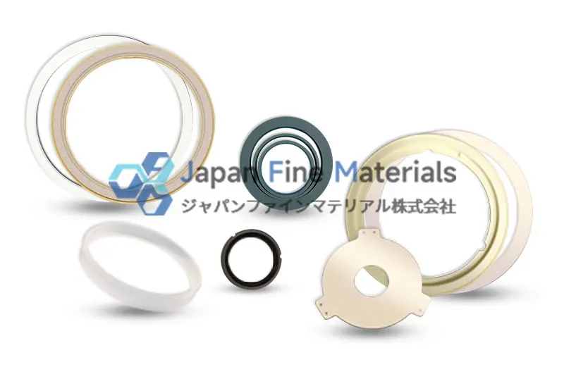
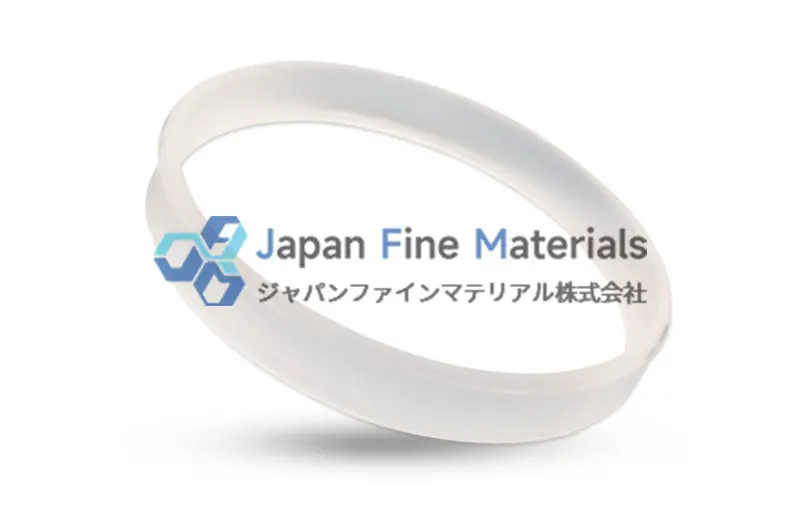
Ceramic Shielding Rings: Protecting Equipment and Improving Wafer Yield
-
2026-04-14 Industry News


Ceramic shielding rings play a critical role in protecting process equipment from plasma and thermal damage while helping stabilize process conditions to improve wafer yield in advanced semiconductor manufacturing.
Introduction
In modern semiconductor manufacturing, the wafer processing environment is extremely harsh. Process steps such as plasma etching, chemical vapor deposition (CVD), and high-temperature treatment can cause severe impact and corrosion to internal equipment components and wafer surfaces. Under these conditions, the service life of equipment wear parts and wafer yield become critical factors in ensuring process stability.As a critical annular ceramic component, the ceramic shield ring not only effectively protects the internal structure of the equipment from direct damage but also optimizes the reaction distribution within the process chamber, thereby enhancing the overall quality of wafer processing and the long-term operational stability of the equipment.
Protecting Equipment and Wafers
In critical semiconductor manufacturing processes such as plasma etching, chemical vapor deposition (CVD), and physical vapor deposition (PVD), internal chamber components are constantly exposed to extreme conditions resulting from the combined effects of high-energy ion bombardment, free radical impact, and corrosive gas environments. Without effective protection, this leads to accelerated wear of electrodes, wafer carriers, and chamber walls, as well as the generation of microparticles that contaminate the wafers.
Ceramic shielding rings, with their high density and other properties, create a stable barrier in critical areas. Their specific functions include:
• Isolating plasma and free radical impacts: Effectively mitigating physical erosion and chemical damage to the surfaces of critical components.
• Reducing the risk of particle contamination: Minimizing the shedding of fine metal and ceramic particles, preventing wafer temperature fluctuations, and protecting the integrity of wafer edges and surfaces.
• Chemically inert material: Does not react with highly reactive gases, reducing byproduct formation and localized corrosion.
• High thermal stability: Maintains structural integrity even in high-temperature environments, ensuring long-term reliable operation of the equipment.
This comprehensive mechanism not only helps extend the service life of core components but also maintains a clean and stable wafer processing environment, laying a solid foundation for high-precision, high-consistency semiconductor manufacturing processes.
Optimizing Process Uniformity
The design of the shield ring directly influences the gas flow field, electric field distribution, and plasma density uniformity within the chamber, thereby having a decisive impact on etch rates and the distribution of film deposition thickness. By precisely optimizing parameters such as ring height, thickness, edge curvature, and surface roughness, edge effects can be effectively mitigated, thereby enhancing the consistency of wafer processing.
• Balancing Plasma Energy: Through structural adjustments, the plasma density at the wafer edges is made consistent with that in the central region.
• Optimizing Gas Flow Distribution: Reducing turbulence and dead zones to improve the overall uniformity of etching or deposition.
• Compatibility with Large-Size Wafers: The benefits are particularly significant for 300mm and larger wafers in multi-layer deposition and complex etching processes.
• Ensuring process repeatability: Guarantees high stability in film thickness and etch depth during long-term production.
Through these design optimizations, the ceramic shield ring has become one of the core technological components ensuring wafer yield and process consistency.
Particle Contamination Control and Yield Improvement
In semiconductor manufacturing, particle contamination at the micron or even nanometer scale can lead to wafer scrap or device performance degradation. Through the use of high-density materials and a chemically inert design, ceramic shield rings effectively reduce particle release and byproduct generation, thereby improving wafer yield.
• Reduced Particle Release Rate: High-density ceramic materials effectively minimize particle shedding caused by plasma erosion or thermal expansion.
• Suppression of Chemical Byproducts: Surface inertness reduces deposits and corrosion products generated by gas reactions.
• Strong Adaptability to Advanced Process Nodes: For more precise processes such as 7 nm, 5 nm, and 3 nm, ceramic shield rings can reduce the risk of device defects caused by particle contamination.
• Maintaining chamber environment stability: Maintains the balance of gas flow, electric field, and plasma density, ensuring process repeatability.
These features have elevated shield rings beyond basic protective components, making them a critical engineering solution for enhancing overall process stability and product yield.
Extended Service Life and Reduced Production Costs
High-performance ceramic shielding rings are specifically designed to withstand the extreme environments of semiconductor manufacturing, including high temperatures, strong corrosion, and high-energy plasma impacts. Their excellent thermal shock resistance and chemical inertness ensure long-term stability under harsh process conditions, extending equipment lifespan and optimizing operating costs.
• Superior Durability: Maintains structural and performance stability even in high-temperature and corrosive environments.
• Reduced Maintenance Frequency: Extended service life minimizes production downtime and maintenance costs.
• Improved Wafer Line Efficiency: Ensures the continuity and stability of the manufacturing process by reducing wafer scrap and production interruptions caused by component failure or contamination.
• Optimized Overall Costs: Reduces the manufacturing cost per wafer by improving process yield and overall equipment utilization.
Through optimized material selection, structural design, and surface treatment, high-performance ceramic protective rings have become indispensable core components in semiconductor manufacturing, enhancing process stability, reducing contamination risks, and controlling operational costs.
Thanks to continuous optimization in materials science, structural mechanics, and surface engineering, high-performance ceramic shielding rings have evolved from basic components into key technological elements for enhancing semiconductor process stability, reducing contamination risks, and controlling operational costs.
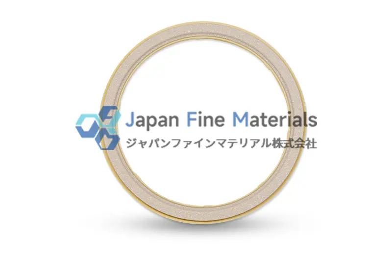
Advantages of Shield Ring Materials and Design
In semiconductor processing equipment, the choice of shield ring materials has a critical impact on high-temperature resistance, corrosion resistance, wear resistance, and the stability of plasma processes.Currently, ceramic materials widely adopted in the industry include alumina, silicon carbide, and zirconia, which demonstrate excellent comprehensive performance across various process scenarios. Additionally, to meet increasingly complex process requirements—such as higher-power plasma environments or stricter cleanliness standards—other high-performance ceramic materials are also selected for specific applications, for example:
|
Material |
Corrosion Resistance |
Wear Resistance |
Electrical Insulation |
Features and Applications |
|
Alumina (Al₂O₃) |
High |
Medium |
Excellent |
Cost-effective and widely used in general plasma etching and chemical vapor deposition processes |
|
Silicon carbide (SiC) |
Extremely high |
High |
Liang |
Suitable for high-energy plasma and highly corrosive gas environments, with a long service life |
|
Zirconia (ZrO₂) |
High |
High |
Excellent |
Excellent thermal stability; suitable for deposition or etching processes requiring high temperature uniformity |
|
Aluminum nitride (AlN) |
High |
Moderate |
Good |
High thermal conductivity, suitable for processes with strict thermal management requirements |
|
Silicon nitride (Si₃N₄) |
High |
Extremely high |
Good |
High mechanical strength and excellent thermal shock resistance, suitable for high-load etching environments |
|
Yttrium oxide (Y₂O₃) |
High |
High |
Excellent |
Excellent thermal cycling stability, suitable for processes with frequent temperature fluctuations |
Furthermore, surface coating technologies (such as oxide, nitride, or chemically resistant coatings) can further enhance the shield ring’s resistance to plasma erosion and chemical corrosion. The selection of coatings must be systematically matched to the substrate material, taking into account key process parameters such as wafer size, plasma power, etch or deposition rates, and equipment model. Through this synergistic optimization, excellent process uniformity and equipment protection can be achieved.
 |
 |
 |
| Aluminum Oxide | Aluminum Oxide | Aluminum Oxide |
 |
 |
 |
| Quartz | Yttrium Oxide Coating | Silicon carbide |
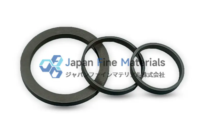
Custom Design
In semiconductor manufacturing, shield rings require highly customized designs to accommodate different wafer sizes, etch rates, and deposition conditions. Through systematic optimization of their dimensions, materials, and structures, these rings can effectively meet specific process requirements, thereby improving wafer uniformity and extending equipment lifespan.
Dimensional and Structural Optimization
Key dimensions of the shield ring—including inner diameter, outer diameter, ring height, and thickness—must be precisely matched to the wafer size and chamber structure to ensure uniform gas flow and plasma distribution within the chamber, thereby preventing etching anomalies or deposition non-uniformity in edge regions. Furthermore, optimizing the cross-sectional shape or incorporating specific tapered designs can effectively guide gas flow paths, enhancing process consistency and stability.
Materials and Surface Treatment
Based on the corrosiveness, temperature, and plasma intensity of the actual process environment, high-performance ceramic materials such as Al₂O₃, SiC, and ZrO₂ can be selected. Furthermore, applying surface coatings such as nitrides and oxides can further enhance corrosion and wear resistance. Optimized surface treatment can also effectively reduce the risk of particle shedding, ensuring wafer yield and extending component service life.
Process Parameter Matching
The design of the shield ring must be coordinated with key process parameters (such as equipment power, operating pressure, and gas flow rate) to achieve optimal plasma distribution and process results. In complex processes involving large-size wafers or multi-layer stacks, customized shield rings can significantly improve wafer-wide uniformity, thereby increasing yield, reducing maintenance frequency, and providing stable and reliable support for semiconductor mass production.
Conclusion
In high-precision plasma etching processes, controlling etch uniformity at the edges of large-size wafers poses a major challenge. Through customized design, high-performance ceramic shield rings can effectively optimize plasma distribution and gas flow patterns in the edge regions, thereby reducing edge defect rates and extending equipment maintenance intervals, which directly improves production efficiency and cost-effectiveness.
In chemical vapor deposition (CVD) applications, shield rings are critical for ensuring the thickness uniformity of deposited films. They not only protect the chamber walls and core components from corrosion by reaction gases and byproducts but also help maintain long-term process stability, providing a reliable foundation for improving wafer yield.
If you are committed to comprehensively improving the process uniformity of semiconductor equipment, extending equipment lifespan, and optimizing overall operating costs, we can provide you with professional, high-performance custom ceramic shield ring solutions. Contact us today to let us help you achieve more efficient and stable wafer manufacturing!


