What is a Wafer Chuck? Why is it so important?
-
2026-04-14 Industry News


A Wafer Chuck is a precision vacuum gripping component used to safely handle semiconductor wafers. This article explains its structure, working principle, and role in maintaining wafer integrity during automated processing.
Introduction
In semiconductor manufacturing, wafers must be precisely secured and stably supported during processes such as lithography, etching, ion implantation, grinding, and polishing. Even deviations on the micrometer scale can lead to a decrease in chip yield. As a critical component of wafer manufacturing equipment, the wafer chuck plays a vital role in securing, positioning, and supporting wafers.With the continuous advancement of cutting-edge processes, ceramic wafer chucks have gradually become a widely adopted solution in the industry due to their excellent comprehensive performance advantages.
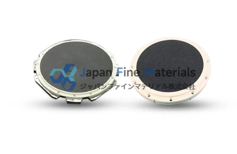
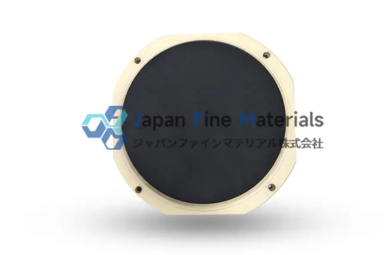
What is a Wafer Chuck?
A wafer chuck, also known as a wafer support platform, is a key component in semiconductor manufacturing equipment used to secure and support wafers. In every stage of wafer processing—whether lithography, etching, thin-film deposition, or chemical mechanical polishing—the wafer must remain highly stable; otherwise, even the slightest deviation can affect chip yield and performance.
Simply put, a wafer chuck acts as a "stage" for the wafer, ensuring it remains rock-solid during precision processes while preventing warping, slipping, or contamination. It not only provides mechanical clamping but also safeguards the wafer in high-temperature, high-pressure, or highly corrosive environments through its material and structural design.
As semiconductor processes continue to advance toward smaller nodes, with wafer sizes and process precision constantly improving, the importance of wafer chucks has become increasingly prominent. High-performance wafer chucks not only improve production yield but also extend equipment lifespan and reduce maintenance costs, making them an indispensable key component for wafer fabs and equipment manufacturers.
Types and Working Principles
The function of a wafer chuck is to securely and damage-free hold the wafer during the semiconductor manufacturing process, ensuring that the wafer does not shift or sustain damage during processes such as lithography, etching, polishing, and inspection. Based on the method of fixation, they are typically classified into three types:
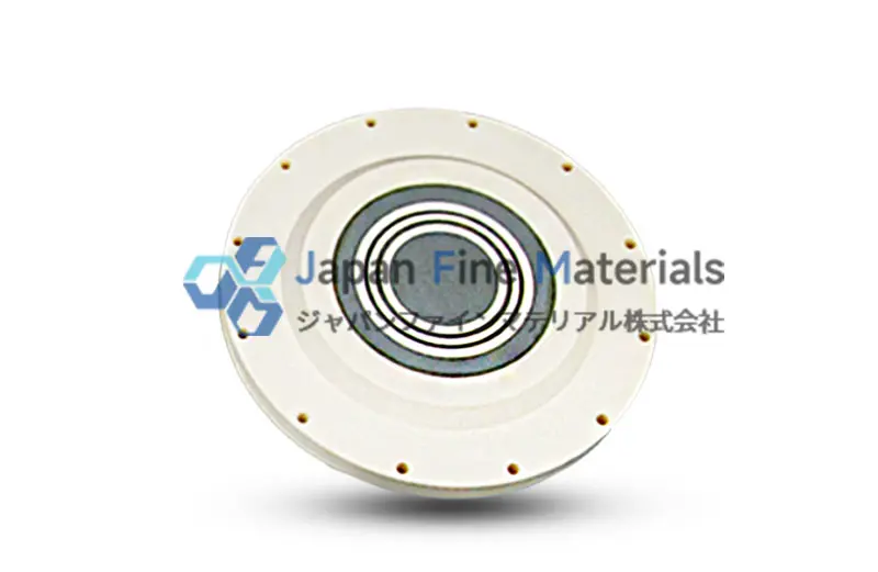
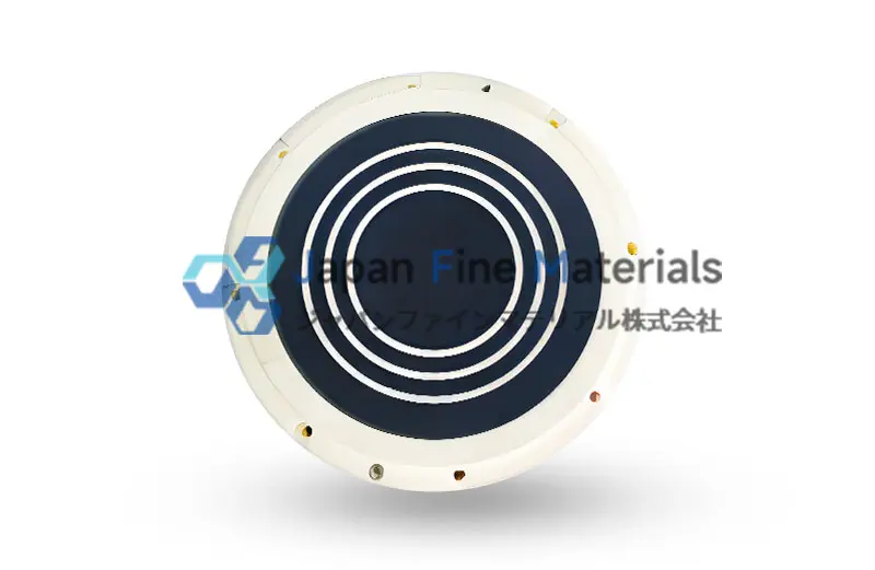
Vacuum Wafer Chucks
Vacuum suction creates a negative pressure on the surface of the wafer carrier, firmly adhering the wafer to the platform. This method is suitable for processes such as polishing, grinding, and inspection that do not have strict temperature requirements but demand stable support, ensuring the wafer remains flat and accurately positioned during operation.
Electrostatic Wafer Chuck Chuck (ESC)
Electrostatic adhesion works by releasing an electric charge through electrodes inside the wafer carrier, generating an electrostatic force between the wafer and the surface to secure the wafer in place. Electrostatic chucks can maintain wafer stability in high-temperature environments, making them widely adopted in advanced processes such as lithography, etching, and thin-film deposition.
Mechanical Wafer Chuck
Mechanical clamping secures the wafer using physical clamps or edge rings. Although structurally simple, this method may exert slight pressure on the wafer edges, so it is primarily used for special testing or small-batch production.
In addition to the clamping method, wafer chuck design also focuses on wafer flatness, thermal management, and cleanliness. A flat surface ensures precise alignment of the wafer in nanoscale processes; thermal management designs maintain stable wafer temperatures; and high-purity materials and structures prevent damage to the wafer caused by particle contamination or electrostatic discharge.
Core Advantages of Ceramic Wafer Chucks
Excellent Thermal Stability
Ceramics maintain dimensional and performance stability under both high and low temperatures, ensuring precise wafer positioning during high-temperature processes or those with drastic temperature fluctuations, such as etching, deposition, and ion implantation. This significantly reduces the risk of wafer warping or misalignment.
Superior Electrical Insulation Properties
Ceramic materials inherently possess insulating properties, which help reduce electrical interference during processes. This is particularly crucial in steps such as plasma etching and ion implantation, where they protect wafers from electrostatic damage.
High Wear and Corrosion Resistance
With high surface hardness and strong chemical stability, ceramic materials maintain consistent performance and surface quality even after prolonged exposure to corrosive gases or frequent wafer loading and unloading. This not only extends the service life of the equipment but also reduces maintenance and replacement costs.
High-Precision Surface Flatness
Ceramics can be machined to achieve high surface flatness and finish, ensuring that wafers adhere tightly during vacuum bonding. This enhances vacuum bonding efficiency while effectively reducing wafer breakage, scratches, and particle contamination.
Lower Risk of Particle Contamination
Compared to metal materials, ceramics are less prone to generating particulate contamination during use. They meet the stringent cleanliness requirements of semiconductor production environments, thereby helping to stabilize yield rates.
Lightweight and structurally robust
Ceramic materials are lighter than other materials but still possess sufficient strength and rigidity. This characteristic helps reduce the load on wafer handling robotic arms or positioning systems, optimizing equipment operational efficiency and stability.
Reliable Performance in Harsh Environments
Whether in high-power plasma environments or ultra-high vacuum chambers, ceramic wafer chucks maintain stable performance and are suitable for advanced manufacturing processes such as EUV lithography and 3D chip fabrication.
Application Scenarios
In the semiconductor manufacturing process, the wafer chuck serves as a critical device for securing and supporting wafers, playing a role across multiple key process steps. Whether in front-end or back-end processes, wafer chucks typically play a vital role in ensuring wafer stability and process reliability. Their performance directly impacts chip yield and final quality. Their function extends beyond mere “securing”; they are a key factor in supporting the stability of high-demand processes.
Lithography
During the lithography stage, the wafer must be secured to the lithography stage with high flatness. The wafer chuck’s suction and support capabilities prevent warping or minute displacement of the wafer, helping to maintain consistent pattern alignment. This is critical for chip manufacturing at advanced process nodes, as even the slightest deviation can lead to circuit failure.
Etching
The etching process requires a high-vacuum environment and stable ion bombardment. A wafer chuck must not only securely support the wafer but also possess excellent resistance to plasma corrosion to prevent material deposition or particle contamination. Additionally, good thermal conductivity ensures that the wafer maintains a uniform temperature distribution during prolonged etching, avoiding localized overheating.
Deposition
During deposition processes such as CVD and PVD, metal or dielectric thin films are deposited onto the wafer surface. Wafer chucks must remain stable in high-temperature, high-energy plasma environments without deformation, while also contributing to the uniformity of film deposition. Their surface design also reduces particle shedding, helping to control yield risks.
Inspection & Metrology
The inspection stage requires precise wafer positioning without vibration to ensure the reliability of results from microscopy and optical inspection. Wafer chucks, using vacuum or electrostatic adhesion, help keep the wafer stationary during inspection, thereby preventing false signals or measurement errors.
Advanced Packaging
With the rise of wafer-level packaging (WLP) and 3D ICs, the application of wafer chucks has expanded from front-end processes to back-end packaging. In this context, they must accommodate the mounting requirements of larger, thinner wafers while mitigating the risk of brittle fracture caused by reduced wafer thickness.
Guide to Selecting Wafer Chucks
When selecting a ceramic wafer chuck, the following factors should be taken into comprehensive consideration to ensure equipment performance and process stability:
Wafer Size and Equipment Compatibility
Selecting a chuck of the appropriate size based on the wafer diameter (e.g., 200 mm, 300 mm) and equipment model helps ensure stable wafer bonding.
Process Type and Environment
Processes such as lithography, etching, thin-film deposition, and CMP have different requirements for the chuck’s thermal stability, corrosion resistance, and electrical insulation. Materials and types (electrostatic chuck or vacuum chuck) should be selected based on the specific process.
Materials and Surface Properties
High-purity ceramic materials provide reliable insulation, corrosion resistance, and a certain level of anti-static performance. Meanwhile, surface flatness and finish affect wafer stability and processing yield.
Service Life and Maintenance Costs
Selecting ceramic chucks with high wear resistance, corrosion resistance, and thermal stability can reduce equipment downtime and maintenance frequency, improve production efficiency, and lower the total cost of ownership (TCO).
Customization Requirements
For special processes or non-standard wafers, ceramic wafer chucks with custom design capabilities can be selected to meet the unique requirements of your equipment and processes.
If you are looking for high-performance, durable, and customizable ceramic wafer chucks, JFM can provide you with expert solutions. Contact us today to receive product support for future-oriented advanced processes and work together to drive the continuous development of the semiconductor industry!
FAQ
Q1: What are the advantages of ceramic wafer chucks over metal ones?
A1: Ceramics offer advantages such as electrical insulation, heat resistance, and corrosion resistance, making them better suited for high-precision processes.
Q2: For which processes can ceramic wafer chucks be used?
A2: They are used in critical stages such as lithography, etching, thin-film deposition, CMP polishing, and wafer inspection.
Q3: Can ceramic wafer chucks be customized?
A3: They can be customized based on wafer size, equipment type, and process requirements.
Q4: What is the approximate service life?
A4: They typically last much longer than metal components, though this depends on the application environment and process conditions.
Q5: Who are the target customers?
A5: Semiconductor equipment manufacturers, wafer fabs, R&D institutions, etc.


