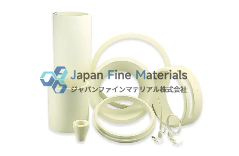
Ceramic Rings for Semiconductor Etching, Deposition, and Ion Implantation
-
2026-04-14 Industry News


Ceramic rings play a critical role in semiconductor etching, deposition, and ion implantation processes, offering excellent thermal stability, chemical resistance, and process reliability in high-precision environments.
I. Introduction
Among the key equipment used in semiconductor manufacturing, precision ceramic rings serve as critical components in multiple core subsystems. Although they do not appear directly in the final product, they have a direct impact on process uniformity, equipment operational stability, and product yield.As processes continue to evolve toward more advanced nodes, the increasing adoption of three-dimensional devices (such as 3D NAND and GAA transistors), along with the iteration of materials and processes such as high-k dielectrics and metal gates, has placed higher demands on the material properties, design and manufacturing precision, and functional integration capabilities of ceramic rings.
II. Core Functions of Ceramic Rings in Semiconductors
Traditionally, ceramic rings have often been viewed merely as “protective components” or “consumables.” However, in modern semiconductor manufacturing, their role has evolved into that of active process control elements, with their functions deeply integrated into the physical aspects of the process.
1. Plasma Management and Uniformity Control
In dry etching, the geometry and surface properties of ceramic rings (such as focus rings) directly influence the formation and distribution of the plasma sheath within the reaction chamber. Optimally designed ceramic rings can precisely regulate the electric field distribution at the wafer edges, compensate for etch rate variations at the wafer edges, and improve process uniformity across the entire wafer.
2. Thermal Management
In chemical vapor deposition (CVD), atomic layer deposition (ALD), and related deposition processes, ceramic rings serve as critical thermal interfaces and support/isolation components. Their thermal conductivity, thermal capacity, and contact thermal resistance with adjacent components influence local temperature distribution and thermal stability, thereby affecting the consistency of film thickness, composition, and properties.
3. Contamination Control and Particle Suppression
The use of high-density ceramic materials with well-controlled porosity and defects, combined with precision machining and surface polishing, reduces the risk of particulate contamination caused by material powdering, flaking, and microcrack propagation. Effective particulate control helps minimize the probability of contamination and supports the cleanliness and consistency requirements of advanced processes.
4. Electrical Insulation and Signal Integrity
In RF plasma processes such as etching, PECVD, and PEALD, ceramic rings are often required to provide stable insulation in RF and high-electric-field environments. They must also work in concert with sensing, monitoring, or matching structures within the chamber to reduce the risk of parasitic discharge and electrical interference, thereby supporting the stability and repeatability of process monitoring.
III. Etching Process Series
1. Focus Ring / Edge Ring
Focus rings and edge rings modulate the sheath potential and ion incidence angle at the wafer edge by precisely controlling the gap, height difference, and dielectric constant relative to the wafer. In etching processes, their design directly affects the uniformity of critical dimensions and etch verticality in the wafer edge region.
2. Cover Ring / Shadow Ring
This is a critical protective component. Through a specific geometric shielding design (shadow effect), it effectively blocks direct bombardment and deposition of plasma or reaction byproducts onto sensitive chamber components (such as the edges of electrostatic chucks and metal hardware). Its contour design typically requires simulation and optimization based on plasma distribution models and line-of-sight analysis to balance protective effectiveness with flow guidance requirements.
3. Chamber Liner / Shield
The chamber liner/shield constitutes one of the key wall surfaces of the reaction chamber. Its material and surface conditions (cleanliness, temperature, roughness, deposition coverage, etc.) influence wall reactions, radical recombination, and deposition/redeposition behavior, thereby affecting etch rates, selectivity, and process stability.Some designs utilize surface topography or structural features to guide deposition adhesion, reduce the risk of flaking, or improve cleaning and maintenance characteristics; however, the specific effects must be evaluated in conjunction with process chemistry and equipment structure.
IV. Deposition Process Series
1. Deposition Ring
In CVD or PVD processes, the primary function of the deposition ring is to shield the wafer edges and backside, preventing backside deposition caused by the diffraction of reaction precursors.Simultaneously, it acts as a thermal and fluidic extension of the wafer periphery, helping to improve the flow field distribution of reaction gases at the wafer edges and the local thermal field uniformity, thereby ensuring film thickness consistency. Its surface material must possess excellent anti-adhesion properties or be easy to clean to withstand periodic chamber cleaning.
2. Gas Distribution Ring/Nozzle Assembly
Some advanced chamber designs integrate gas introduction functions with ceramic rings. Through precision-machined channels or microporous arrays on the ring body, these designs achieve uniform injection or laminar flow control of reaction gases around the wafer periphery. This design plays a crucial role in optimizing gas flow uniformity for large-size wafers and controlling reaction rate distribution, and is commonly used in atomic layer deposition or epitaxial growth equipment requiring high precision in gas flow control.
V. Ion Implantation Process Series
1. Beam Limiting Ring
This component is located along the ion beam transmission path. Through precise aperture design, it collimates and shapes the beam, eliminating stray ions at the edges to precisely define the beam profile for wafer implantation. The inner edge of the aperture must possess extremely high geometric precision and surface finish to minimize ion scattering.
2. High-Voltage Insulator Ring
Used in ion source extraction systems or accelerating tube assemblies, its primary function is to isolate high-voltage potential differences ranging from tens of thousands to hundreds of thousands of volts in a high-vacuum environment. This ceramic ring must possess excellent vacuum dielectric strength and low outgassing rates, and it must withstand X-ray radiation generated by ion beam bombardment without electrical performance degradation. In high-temperature implantation processes (such as SiC device manufacturing), it must also maintain stable volume resistivity under high-temperature conditions.
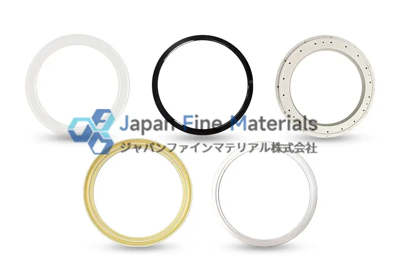
VI. Material Selection and Application Strategies for Ceramic Rings
Material selection is the cornerstone of ceramic ring performance, and different process environments require distinctly different material solutions. The selection process is a multi-objective optimization problem that comprehensively considers chemical compatibility, thermodynamic properties, electrical characteristics, and total cost of ownership (TCO).
1. Alumina (Al₂O₃) Ceramic Rings
Alumina ceramics typically feature high hardness, good mechanical strength, and excellent electrical insulation properties. The manufacturing process is well-established, and costs are relatively controllable. They are commonly used in deposition processes with relatively mild or controllable corrosion conditions (such as certain PVD/CVD processes) and in ion implantation equipment, serving as insulating rings, fixing/support rings, and other structural and insulating components (specific suitability still requires evaluation based on process atmospheres and cleaning chemicals).
2. Aluminum Nitride (AlN) Ceramic Rings
The core advantage of aluminum nitride lies in its high thermal conductivity and thermal expansion coefficient similar to that of silicon wafers. This makes it the preferred choice for applications with extremely high thermal management requirements, such as the main base of electrostatic chucks (ESC), heat spreading plates for high-temperature CVD heaters, and heat dissipation components in high-power process chambers. It effectively eliminates local hot spots and improves wafer temperature uniformity.
3. Yttrium Oxide (Y₂O₃) Ceramic Rings
Yttrium oxide ceramics are commonly used in certain halogen plasma environments (particularly fluorine-containing systems) to enhance resistance to plasma erosion and help reduce the risk of metal contamination and particle-related issues. Consequently, in advanced etching processes, yttrium oxide-based materials (including bulk materials or coating solutions) are often considered as candidates for components such as chamber liners, focusing rings, and shielding/shadow rings.In metal etching and other scenarios sensitive to metal contamination, they are also prioritized for evaluation due to cleanliness and contamination control requirements (depending on the equipment platform and process window).
4、 Silicon Carbide (SiC) Ceramic Rings
Silicon carbide (SiC) ceramic rings combine excellent mechanical strength, wear resistance, and thermal stability, making them suitable for applications requiring high structural rigidity, thermal deformation control, and long-term operational reliability.High-purity silicon carbide (particularly CVD-SiC), due to its dense, non-porous surface characteristics, exhibits excellent resistance to particulate contamination. It is widely used in rapid thermal processing (RTP) and epitaxy equipment as wafer support rings, capable of withstanding severe thermal stress without deformation; furthermore, in specific etching processes, it is also used as a highly wear-resistant focusing ring material to replace traditional silicon rings and extend maintenance intervals.
Material Selection Guide
|
Process Environment |
Recommended Material |
Key Considerations |
|
General Deposition / Ion Implantation |
High-purity alumina (Al₂O₃) |
Cost-effective, excellent insulation properties, good mechanical strength |
|
High Thermal Conductivity / Thermal Management Components |
Aluminum Nitride (AlN) |
High thermal conductivity, low coefficient of thermal expansion, excellent thermal uniformity |
|
Highly Corrosive Plasma Etching |
Yttrium Oxide (Y₂O₃) |
Good erosion resistance, low volatility of byproducts, low risk of particle contamination |
|
High-temperature thermal shock / Epitaxial processes |
Silicon carbide (SiC) |
Excellent thermal shock resistance, extremely high rigidity, high-purity dense surface |
VII. Conclusion
As semiconductor manufacturing processes continue to evolve, higher demands are placed on the material properties, cleanliness control, and long-term stability of critical components. For highly specialized components such as ceramic rings, the optimization of material systems, the synergistic design of structure and function, and process adaptation to specific equipment platforms are increasingly becoming key factors in expanding process windows, ensuring stable mass production performance, and enhancing the overall competitiveness of equipment.
With the development of advanced processes, three-dimensional device structures (such as 3D NAND and GAA), and diverse pathways including compound semiconductors and power devices, relying solely on standard components often fails to meet the differentiated requirements across different process windows.Collaborative development and iterative validation based on a deep understanding of the process can more effectively balance requirements across dimensions such as plasma erosion resistance, thermal management, particle control, electrical insulation, and assembly consistency, thereby reducing implementation risks and enhancing long-term operational stability and cost-effectiveness.
JFM offers high-purity precision ceramic rings and related components made from materials such as alumina, yttria, aluminum nitride, and silicon carbide. We provide tailored recommendations for material selection, structural design, and manufacturing processes based on specific operating conditions and design constraints, supporting the development and validation of functionally integrated components. Please contact the JFM technical team to initiate a customized evaluation of ceramic components tailored to your equipment and process requirements.


