Conductive Ceramic Arm Applications in Semiconductor Manufacturing
-
2026-09-09 Industry News






Learn about conductive ceramic arm applications in semiconductor manufacturing, including wafer handling, key properties, and equipment integration.
Introduction
As semiconductor manufacturing processes continue to evolve toward greater precision, the requirements for component materials in production equipment are also gradually increasing. In processes such as wafer processing, inspection, and handling, internal equipment components must meet demands for high cleanliness, high precision, and complex process environments.
As one of the key precision components in semiconductor equipment, the Conductive Ceramic Arm—leveraging the unique properties of ceramic materials—is used in wafer-handling robots, vacuum equipment, and automated manufacturing systems. Compared to traditional metal structures, the Conductive Ceramic Arm offers certain advantages in terms of material characteristics, electrical performance control, and adaptability to cleanroom environments, making it a component solution of interest to some semiconductor equipment manufacturers.
This article will introduce the structural features, material advantages, and primary application scenarios of the Conductive Ceramic Arm in semiconductor manufacturing, helping equipment manufacturers and procurement personnel better understand this precision ceramic component.
What Is a Conductive Ceramic Arm?
A Conductive Ceramic Arm is a precision robotic arm component manufactured from conductive ceramic materials, typically used in equipment systems that require high cleanliness and precise motion control.
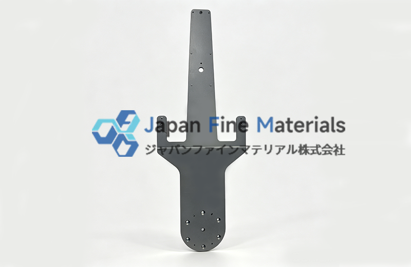
During the semiconductor manufacturing process, wafers undergo multiple processing steps, including:
• Wafer transfer
• Photolithography
• Etching
• Thin-film deposition
• Inspection and Measurement
Since wafer surfaces are highly sensitive to contamination, particles, and mechanical damage, internal handling components within the equipment must possess good dimensional stability and material compatibility.
Conductive ceramic arms are typically machined from aluminum oxide-based conductive ceramics, silicon carbide ceramics, or other composite ceramic materials. By adjusting the material formulation, they are given certain electrical conductivity while retaining the ceramic material’s inherent characteristics, such as heat resistance, wear resistance, and low particle release.
Why Are Conductive Ceramic Arms Used in Semiconductor Manufacturing?
In semiconductor production environments, equipment components must not only meet mechanical motion requirements but also address electrostatic control, cleanliness, and long-term performance during the manufacturing process.
The use of Conductive Ceramic Arms in semiconductor equipment is primarily related to the following aspects:
Electrostatic Control Requirements
During the semiconductor manufacturing process, static electricity may accumulate between wafers and equipment components. In certain precision manufacturing stages, static electricity can interfere with wafer processing; therefore, equipment designs typically incorporate materials with conductive properties to manage static discharge.
Although traditional insulating ceramics offer excellent insulation properties, certain application environments require materials with controllable conductivity.
Through material design, the Conductive Ceramic Arm ensures that its resistivity characteristics fall within a range suitable for equipment applications, providing a material option for electrostatic control solutions in semiconductor equipment.
Suitable for High-Cleanliness Manufacturing Environments
Semiconductor manufacturing imposes stringent requirements on the cleanliness of the production environment, and internal equipment components must minimize particle generation as much as possible.
Compared to some metallic materials, ceramic materials offer superior corrosion resistance and surface stability, making them valuable for use in vacuum equipment and clean manufacturing environments.
During the design process of the Conductive Ceramic Arm, the following aspects are typically considered:
• Surface machining precision
• Material purity
• Edge treatment methods
• Particle control during use
These factors all affect the component’s performance in semiconductor equipment.
Meeting Precision Motion Requirements
Wafer handling equipment typically requires high-frequency, repetitive, and precise motion; therefore, robotic arm components must possess excellent dimensional stability.
Ceramic materials have low thermal expansion properties, which help minimize the impact of dimensional changes on motion accuracy in equipment environments with significant temperature fluctuations.
For semiconductor equipment manufacturers, selecting the appropriate ceramic arm material can help optimize equipment structural design and improve operational consistency.
Applications of Conductive Ceramic Arms in Semiconductor Manufacturing
Conductive ceramic arms are not standalone functional components; rather, they serve as precision transfer and support components within semiconductor equipment, working in conjunction with robotic systems, vacuum chambers, and automated control systems to complete the wafer handling process.
Wafer Handling Equipment
Wafer handling equipment is a critical component of semiconductor production lines, primarily responsible for transferring wafers between different process equipment.
In the automated wafer manufacturing process, robotic arms must frequently perform the following tasks:
• Wafer Gripping
• Wafer positioning
• Wafer transfer
• Transfer between process chambers
As wafer sizes continue to increase and manufacturing precision requirements continue to rise, handling components must balance lightweight design, structural strength, and cleanliness.
Conductive Ceramic Arms are typically mounted at the end effector of wafer robots; they are precision-machined to meet the structural dimensional requirements of the equipment and are used to support wafers during the transfer process.
The material properties make them suitable for equipment environments with specific requirements for particle control, electrical performance, and thermal stability.
Vacuum Semiconductor Equipment
Many semiconductor manufacturing processes must be performed in a vacuum environment, such as:
• PVD (Physical Vapor Deposition)
• CVD (Chemical Vapor Deposition)
• Etching
• Ion implantation
Inside these devices, components are exposed to vacuum environments, temperature fluctuations, and the effects of chemical gases.
Conductive Ceramic Arms, due to their excellent heat resistance and chemical stability, are used in certain vacuum transport systems and internal chamber structures.
Compared to some traditional materials, ceramic components exhibit relatively minimal changes in material properties in high-temperature process areas, helping to meet the demands of equipment designs for precision motion components.
Semiconductor Robotic Systems
Semiconductor robotic systems have high requirements for motion precision and repeatable positioning capabilities.
As a critical component of the robot’s end-effector, the ceramic arm must meet the following requirements:
• Precise dimensional control
• Lightweight design
• Good mechanical strength
• Compatibility with the equipment control system
Conductive ceramic materials combine the mechanical properties of ceramics with electrical conductivity, offering a viable component option for semiconductor automation equipment.
In practical applications, manufacturers typically customize the design of ceramic arms based on robot structure, wafer size, operating temperature, and the equipment environment.
Semiconductor Testing Equipment
In addition to manufacturing process equipment, inspection equipment also requires high-precision wafer handling components.
During the wafer inspection process:
• Wafers must be kept precisely positioned
• The handling process must minimize mechanical impact
• A clean environment must be maintained inside the equipment
The Conductive Ceramic Arm can be used in the wafer transfer structures of certain inspection systems, providing a material solution for equipment design.
Conductive Ceramic Arm vs. Traditional Metal Arms
In the design process of semiconductor equipment, material selection directly impacts the performance of components. Conductive Ceramic Arms and metal arms each have their own characteristics, and the choice depends on the specific requirements of the equipment.
|
VS |
Conductive Ceramic Arm |
Metal Arm |
|
Material Type |
Conductive Ceramic Materials |
Metal materials such as aluminum alloy and stainless steel |
|
Weight Characteristics |
Typically have a lower density |
Varies depending on the type of metal |
|
Thermal Expansion Properties |
Minimal thermal dimensional changes |
Some variation exists among different metals |
|
Chemical stability |
Good adaptability to certain corrosive environments |
Depends on the type of metal and surface treatment |
|
Electrical conductivity |
Can be adjusted through material design |
Metals are inherently conductive |
|
Applications |
Semiconductors, vacuum systems, precision equipment |
General-purpose mechanical structures, automation equipment |
It is important to note that there is no fixed approach to material selection. In actual projects, engineering teams typically conduct a comprehensive evaluation that takes into account equipment structure, process conditions, and cost requirements.
Manufacturing Process for the Conductive Ceramic Arm
Conductive Ceramic Arms are precision ceramic components, and their production process typically involves multiple stages, including material preparation, forming, sintering, and precision machining.
Raw Material Preparation
Advanced ceramic manufacturers select appropriate ceramic material systems based on product application requirements, such as:
• Conductive alumina ceramics
• Silicon carbide ceramics
• Composite ceramic materials
The material formulation affects the product’s electrical conductivity, mechanical properties, and processing characteristics.
Ceramic Molding
After the ceramic powder is mixed, it must undergo a forming process to create the initial structure.
Common forming methods include:
• Dry pressing
• Injection Molding
• Slip Casting
Different structural dimensions and product requirements call for different manufacturing solutions.
Sintering Process
Sintering is a critical step in ceramic manufacturing. Common ceramic sintering methods include:
• Atmospheric Sintering: This method promotes the densification of ceramic materials through a high-temperature environment and is commonly used in the manufacture of certain ceramic components;
• Hot-press sintering: Applying pressure simultaneously during the heating process helps improve material density; this method is suitable for certain high-performance ceramic materials;
• Reaction Sintering: Forms ceramic structures through chemical reactions; this method is commonly used for specific material systems.
Through high-temperature treatment, the particles within the ceramic material bond together, giving the product the desired structural properties.
Temperature control, atmospheric conditions, and time parameters during the sintering process all affect the final product quality.
Precision Machining and Inspection
After sintering is complete, Ceramic Arm typically requires the following:
• CNC Precision Machining
• Surface treatment
• Dimensional inspection
• Resistance Testing
• Visual inspection
For semiconductor applications, dimensional tolerances and surface quality are critical factors affecting component performance.
How to Select the Right Conductive Ceramic Arm?
In semiconductor manufacturing equipment, conductive ceramic arms must be selected based on specific application scenarios . Different equipment has varying requirements for material properties, structural dimensions, and machining precision; therefore, a comprehensive evaluation of multiple factors is necessary during the selection process.
Selecting the Right Ceramic Material
The type of material used in a Conductive Ceramic Arm directly affects the product’s electrical conductivity, mechanical strength, and adaptability to the operating environment.
Common materials include:
• Conductive alumina ceramic: Offers good overall performance and is suitable for precision structural components in certain semiconductor equipment
• Silicon carbide ceramics: Offer good heat resistance and wear resistance, making them suitable for certain applications requiring high temperature resistance and material stability
• Composite conductive ceramics: Material properties can be adjusted according to equipment requirements
When selecting materials, an evaluation must be conducted based on the equipment’s operating temperature, electrical requirements, and actual application conditions.
Consider Product Structure and Dimensions
Conductive Ceramic Arms are typically used in conjunction with robotic systems or wafer transfer mechanisms in semiconductor equipment; therefore, matching the product structure and dimensions is critical.
Key considerations during selection include:
• Ceramic Arm length and overall dimensions
• Mounting interface design
• Wafer size compatibility
• Equipment motion space requirements
A well-designed structure helps components better meet equipment operational requirements while reducing the difficulty of adjustments during installation.
Focus on Precision Machining Quality
Since semiconductor manufacturing processes demand high precision, Conductive Ceramic Arms typically require precision machining.
When selecting products, focus on:
• Dimensional Tolerance Control
• Surface roughness
• Machining consistency
• Appearance quality
Good machining processes help improve the fit between components and equipment and meet the application requirements of precision manufacturing environments.
Adaptation to Practical Application Environments
Operating conditions vary among different semiconductor equipment—such as wafer handling systems, vacuum chamber systems, and inspection equipment—and the requirements for ceramic components also differ accordingly.
When selecting a Conductive Ceramic Arm, consider the following:
• Whether it will be used in a vacuum environment
• Whether high-temperature processes are involved
• Whether electrostatic effects need to be controlled
• Whether cleanroom manufacturing requirements must be met
Selecting the appropriate product solution based on the specific application environment will help ensure that the Conductive Ceramic Arm better meets the equipment’s requirements.
Conclusion
In the semiconductor manufacturing process, the choice of materials for precision components influences equipment design and production processes. As a ceramic component used in wafer handling, vacuum equipment, and automation systems, the Conductive Ceramic Arm has become a critical component in certain semiconductor equipment due to its conductive properties, material stability, and precision machining capabilities.
For equipment manufacturers, selecting a Conductive Ceramic Arm requires a comprehensive evaluation based on actual application scenarios, taking into account factors such as material type, machining capabilities, dimensional requirements, and supplier technical support.
JFM specializes in the R&D and manufacturing of precision ceramic components, providing customized products such as Conductive Ceramic Arms and ceramic structural parts for the semiconductor equipment industry. Leveraging its expertise in material processing and well-established manufacturing processes, JFM offers comprehensive services—from material selection and product design to precision machining—tailored to customer needs, helping clients develop ceramic component solutions that meet their equipment application requirements.
If you are looking for a supplier of Conductive Ceramic Arms for semiconductor equipment, please contact JFM to learn more about our products and customized solutions.