Electrostatic Chucks For Semiconductor Wafer Processing
-
2026-09-09 Industry News






Explore how electrostatic chucks support semiconductor wafer processing, including wafer holding, temperature control, plasma processes, and key design considerations.
Introduction
In the semiconductor manufacturing process, wafers undergo multiple processing steps, including etching, thin-film deposition, and ion implantation. During processing, the wafer’s position, temperature, and contact with the equipment all affect the process.
An electrostatic chuck is a precision component used to hold wafers. It secures the wafer using electrostatic forces and can incorporate features such as back-side gas flow, heating structures, and multi-zone electrodes, depending on the equipment design.
For semiconductor equipment, an electrostatic chuck is more than just a simple wafer-holding component; its materials, electrode structure, surface topography, and thermal management design are all closely tied to specific processes.
So, what specific role does an electrostatic chuck play in semiconductor wafer processing? What are its common applications? And what are the differences between various materials?
What Is a Semiconductor Electrostatic Chuck?
A semiconductor wafer electrostatic chuck is a precision clamping component that secures wafers using electrostatic forces.
Unlike mechanical fixtures, which clamp wafers using physical pressure, an electrostatic chuck applies a voltage through internal electrodes to create an electric field between the chuck and the wafer, generating a holding force through electrostatic interaction.
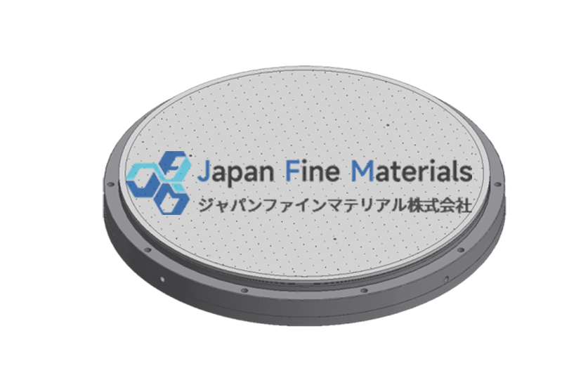
A typical electrostatic chuck usually consists of:
• A ceramic substrate
• Internal electrodes
• Wafer-bearing surface
• Back-side gas channels
• Heating structure
• Mounting structure
The specific structure is adjusted based on wafer size, manufacturing processes, and semiconductor equipment requirements.
In practical applications, the electrostatic chuck not only secures the wafer but may also be involved in wafer temperature control and back-side gas management; therefore, its design must be compatible with the entire process system.
How does an electrostatic chuck hold a semiconductor wafer in place?
The core of an electrostatic chuck is the electrostatic field generated by its internal electrodes.
When a wafer is placed on the chuck’s surface, the equipment applies a voltage to the internal electrodes. The electric field creates an electrostatic interaction between the wafer and the electrodes, causing the wafer to be attracted toward the chuck’s surface.
The basic operating process can be summarized as follows:
1. Wafer placement
2. Voltage is applied
3. Generation of an electric field
4. Formation of electrostatic attraction
5. The wafer is held on the suction cup surface
The electrostatic adhesion mechanism varies depending on the electrode structure and ceramic material.
Common electrostatic chucks can employ either a unipolar or bipolar structure. In bipolar electrostatic chucks, the positive and negative electrodes are typically positioned in different areas to optimize the electric field distribution for the specific equipment design.
Once wafer processing is complete, the de-adhesion process begins. This involves reducing the voltage or discharging residual charges to allow the wafer to separate from the chuck surface.
Why Do Semiconductor Equipment Use Electrostatic Chucks?
Semiconductor processes are highly sensitive to wafer position, temperature, and surface cleanliness.
Particularly in vacuum processes such as plasma etching, PECVD, and PVD, any significant change in the contact between the wafer and the mounting platform can affect local wafer temperature and process uniformity.
The value of an electrostatic chuck lies not merely in “holding the wafer in place,” but in integrating wafer clamping, heat transfer, and equipment structure into a single functional component.
Compared to some traditional clamping methods, it has several distinct features:
• Non-mechanical edge clamping: No large-area mechanical clamping structures are required on the wafer surface, which helps minimize interference from the clamping mechanism with the process area.
• Compatibility with vacuum equipment: Electrostatic adhesion does not rely on the environmental pressure differential required by traditional vacuum chucks, making it more suitable for certain vacuum semiconductor equipment.
• Facilitates wafer temperature management: Once a relatively uniform contact is established between the wafer and the electrostatic chuck, more precise thermal management can be achieved by combining internal cooling structures with back-side gas flow.
• Facilitates integration of other equipment functions: Electrostatic chucks can be integrated with heaters, cooling channels, RF electrodes, He gas channels, lift pins, and other structures.
Consequently, in modern wafer processing equipment, the electrostatic chuck functions more as a comprehensive wafer-holding platform rather than merely a simple fixture.
Major Applications of Electrostatic Chucks in Wafer Processing
Plasma Etching
Plasma etching is one of the most typical applications for electrostatic chucks.
During the etching process, the wafer must be held in a specified position and maintained in a controlled plasma environment. The electrostatic chuck secures the wafer via electrostatic forces while managing thermal conditions through integrated back-side gas and temperature control systems.
Physical Vapor Deposition
In thin-film deposition processes such as PVD, the wafer must be maintained in the correct position and orientation.
Electrostatic chucks can serve as wafer-holding and clamping components, and temperature management functions can be incorporated based on the equipment design.
Depending on the deposition materials and process conditions, the ceramic materials, electrode structures, and surface designs used in electrostatic chucks may vary.
Chemical Vapor Deposition
During the CVD process, wafers must be maintained at a specific temperature and within a specific reaction environment.
Some electrostatic chucks can be integrated with heating structures to provide temperature control for the wafer. At the same time, the flatness and thermal conductivity of the chuck surface must be evaluated in accordance with process requirements.
Ion Implantation
During the ion implantation process, the wafer must be positioned according to the equipment’s process requirements.
Electrostatic chucks can secure wafers using electrostatic forces and, in conjunction with the equipment structure, contribute to wafer temperature management.
Since the ion implantation process involves high-energy particles, the material, electrical structure, and temperature resistance of the electrostatic chuck must be selected based on the specific equipment.
Wafer Inspection and Measurement
Some wafer inspection and measurement equipment also requires precision wafer-holding structures.
In such applications, an electrostatic chuck can be used to secure the wafer in place; however, the decision to use an ESC must be based on the operating environment of the inspection equipment, wafer surface requirements, and positioning accuracy.
Common Materials for Semiconductor Electrostatic Chucks
Material selection is a critical aspect of electrostatic chuck design. Currently, common materials used for ceramic electrostatic chucks in semiconductor equipment include aluminum oxide and aluminum nitride.
Aluminum Oxide Electrostatic Chucks
Alumina possesses excellent electrical insulation, heat resistance, and chemical stability, making it suitable for use in electrostatic chucks in certain semiconductor equipment.
The specific properties of alumina are influenced by its purity, composition, and manufacturing process.
When selecting an alumina electrostatic chuck, in addition to considering the material name, it is necessary to evaluate factors such as volume resistivity, dielectric properties, coefficient of thermal expansion, and surface roughness.
Aluminum Nitride Electrostatic Chucks
Aluminum nitride has high thermal conductivity and electrical insulation properties, making it a common choice for applications with stringent wafer thermal management requirements.
For example, in processes such as plasma etching, if the equipment requires precise control of wafer temperature, the thermal conductivity of aluminum nitride can provide a material foundation for the design of the chuck structure.
Of course, aluminum nitride is not the default choice for all applications; the final decision still requires evaluation based on specific process conditions.
|
VS |
Aluminum Oxide Electrostatic Chuck |
Aluminum Nitride Electrostatic Chuck |
|
Primary Material |
Al₂O₃ |
AlN |
|
Electrical Insulation |
Good |
Good |
|
Thermal conductivity |
Relatively low |
High |
|
Thermal management capability |
Suitable for general thermal management needs |
Suitable for scenarios with higher thermal management requirements |
|
Common Considerations |
Insulation properties, mechanical properties, material cost |
Thermal conductivity, thermal expansion, electrical properties |
|
Typical Applications |
Various semiconductor equipment |
Equipment with stringent temperature control requirements |
It should be noted that actual product performance is determined not only by the material itself but is also influenced by factors such as ceramic purity, manufacturing process, thickness, electrode structure, and surface finishing.
Back-side Gas in Electrostatic Chucks
In some semiconductor equipment, gases such as helium are introduced to the backside of the wafer—a process commonly referred to as backside gas cooling.
The microscopic gap between the wafer and the surface of the electrostatic chuck (typically controlled by a surface bump structure) serves as a channel for the flow of back-side gas (such as helium). These gas molecules act as a heat transfer medium, and their mean free path must match the gap size to achieve efficient and uniform heat exchange.
The gas facilitates heat exchange between the wafer and the chuck.
Therefore, electrostatic chucks typically require the following structural design elements:
• Gas inlet
• Gas channel
• Distribution area
• Sealing structure
• Surface microstructure
The pressure, flow rate, and distribution of the gas on the back side must be adjusted according to the equipment’s process requirements.
Heating Structure in an Electrostatic Chuck
Some semiconductor electrostatic chucks incorporate heaters for wafer temperature control.
In processes such as etching and deposition, temperature affects material reactions and the fabrication process; therefore, wafer temperature must be controlled according to process conditions.
Heaters are typically located inside the ceramic structure or integrated with the chuck structure, and different heating zones are defined according to equipment requirements.
If a multi-zone heating structure is used, temperatures in different zones can be adjusted according to the equipment design.
During the actual design process, the following factors must be considered simultaneously:
• Heating power
• Temperature uniformity
• Heating zones
• Heat transfer pathways
• Ceramic materials
• Thermal Expansion Differences
These factors are interrelated; therefore, a single temperature parameter cannot be considered in isolation.
The Importance of the Electrostatic Chuck Surface
Since the wafer is placed directly on the surface of the electrostatic chuck, the surface condition affects the contact between the wafer and the chuck.
Key considerations for the electrostatic chuck surface typically include:
• Flatness: Significant deviations in surface flatness may affect the contact between the wafer and the chuck, as well as the distribution of gas on the wafer’s backside.
• Surface Roughness: Surface roughness affects the microscopic contact between the wafer and the chuck and may also influence heat transfer.
• Microstructure: Some electrostatic chucks feature microscopic protrusions or other structures on their surfaces to create spaces for gas flow beneath the wafer.
• Particle Control: Semiconductor processes are highly sensitive to particles; therefore, the machining and cleaning of the electrostatic chuck’s surface must also be incorporated into quality control.
How to Select an Electrostatic Chuck for Semiconductor Wafer Processing?
For semiconductor equipment manufacturers and wafer processing companies, the selection of an electrostatic chuck must be based on actual process requirements.
Selection Based on Wafer Size
First, determine the wafer size, such as 200 mm or 300 mm.
At the same time, confirm the chuck’s outer diameter, effective adhesion area, and equipment mounting dimensions.
Selecting Based on the Processing Technology
Different processes have varying requirements for electrostatic chucks. For example:
• Plasma etching places greater emphasis on temperature control and backside gas;
• PVD may place greater emphasis on material compatibility and surface condition;
• CVD requires attention to the heating structure and heat conduction;
• Ion implantation requires evaluation based on the equipment’s energy and temperature conditions.
Selection Based on Ceramic Materials
If the equipment has stringent thermal management requirements, aluminum nitride should be prioritized for evaluation.
If you are more interested in the overall material performance, you can compare it with materials such as alumina.
Selection Based on Electrode Structure
Single-pole, bipolar, and multi-zone electrode structures each have distinct design characteristics and must be selected based on the equipment’s power supply and process requirements.
Selection Based on Temperature Control Method
If the equipment requires wafer heating, the heater structure, heating zone, power rating, and temperature sensing method must be further confirmed.
Selection Based on Equipment Interfaces
The electrostatic chuck must also be compatible with the equipment’s power supply, gas, vacuum, heating, and mounting systems.
Therefore, when customizing an electrostatic chuck, equipment drawings, wafer dimensions, and process parameters are all important reference information.
Conclusion
The electrostatic chuck is a critical precision component in semiconductor wafer processing equipment. Its core function is to secure the wafer using electrostatic forces and, depending on the equipment design, to perform certain temperature management and back-side gas control functions.
From ceramic materials such as alumina and aluminum nitride to internal electrodes, surface microstructures, heaters, and back-side gas channels, every component affects how well the electrostatic chuck matches a specific semiconductor process.
Therefore, when selecting an electrostatic chuck for semiconductor wafers, a comprehensive evaluation must be conducted that takes into account wafer size, processing technology, materials, electrode structure, temperature requirements, back-side gas, and equipment interfaces.
JFM Electrostatic Chuck Solutions
JFM specializes in the R&D and manufacturing of ceramic components for the semiconductor and precision machining industries. We offer customized electrostatic chuck solutions based on wafer size, ceramic materials, electrode structure, temperature control requirements, and equipment installation conditions.
If you are looking for an electrostatic chuck for semiconductor wafer processing, please feel free to contact us. Provide JFM with your wafer size, processing method, material requirements, technical specifications, or product drawings, and we can discuss suitable product solutions based on your specific application.