What Is Platinum Paste Used for in Semiconductor Packaging?
-
2026-06-29 Industry News






Explore the function of platinum paste in modern semiconductor packaging and how it improves performance in demanding electronic environments.
As semiconductor packaging continues to evolve toward higher frequencies, higher power, and miniaturization, traditional conductive and interconnect materials are no longer sufficient to meet stability requirements under complex operating conditions. Particularly in the fields of automotive electronics, optical communications, power devices, sensors, and advanced packaging, demands for high-temperature resistance, oxidation resistance, conductive stability, and long-term reliability are becoming increasingly stringent.
Against this backdrop, platinum paste has gradually emerged as one of the key materials in high-end semiconductor packaging. Compared to common silver, copper, and gold pastes, platinum paste demonstrates superior performance characteristics in high-temperature and corrosive environments, as well as in terms of long-term stability. As a result, it is widely used in packaging structures that demand extremely high reliability.
So, what exactly are the specific applications of platinum paste in semiconductor packaging? Why is it still indispensable for certain high-end packaging solutions? This article will analyze these questions from the perspectives of material properties, application scenarios, and industry trends.
What Is Platinum Paste?
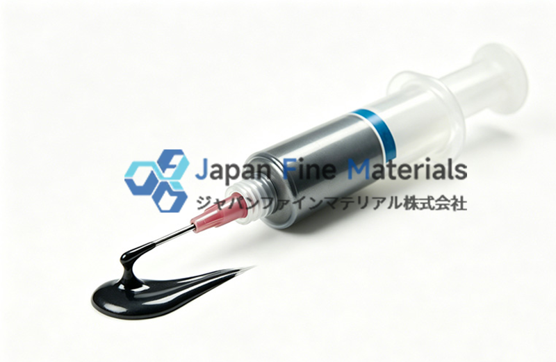
Platinum paste is a thick-film paste composed of a platinum metal functional phase, an inorganic binder phase (typically a glass material such as borosilicate or bismuth-based glass), and an organic carrier system. It is formed via screen printing or dispensing and, after high-temperature sintering (typically >850°C), forms a dense, conductive layer.
In terms of formulation design, this type of material requires a balance between rheological properties and subsequent heat treatment behavior, enabling it to undergo structural transformation under specific process conditions while maintaining a stable physical form.
Generally, the core composition of platinum paste includes the following components:
• Platinum functional phase (provides conductivity and high-temperature resistance)
• Organic carrier system (adjusts the slurry’s rheological properties for screen printing)
• Additives (such as dispersants and thixotropic agents, used to optimize printing and sintering behavior)
Due to the complexity of their formulation, platinum pastes typically require processing under tightly controlled conditions to ensure the consistency and stability of the final structure.
The primary role of platinum paste in semiconductor packaging
High-temperature conductive connections
Many power semiconductor devices generate a significant amount of heat during operation, such as IGBT modules, SiC/GaN power devices, high-power LEDs, and automotive electronic modules.
Conventional conductive materials are prone to oxidation, migration, or performance degradation under prolonged high-temperature conditions. In contrast, platinum has a melting point as high as 1768°C and, in high-temperature oxidizing environments, does not readily form a stable, dense oxide insulating layer. Consequently, the conductive layer formed after sintering platinum paste can maintain relatively low and stable resistivity under high-temperature operating conditions.
As a Thick-Film Electrode Material
In ceramic substrate packaging, platinum paste is frequently used to fabricate thick-film electrodes.
For example:
• Alumina ceramics
• Aluminum nitride ceramics
• LTCC substrates
• HTCC substrates
These substrates typically require sintering at high temperatures, so the temperature resistance of the metal materials is critical.
Platinum paste is typically sintered in the range of 850°C to 1000°C, but the optimal temperature depends on the glass frit composition and substrate type. The sintered layer should exhibit good adhesion and conductivity when properly matched to the specific substrate and paste formulation, while maintaining good electrical conductivity and mechanical bonding strength.
Such applications are particularly common in sensor packaging and RF devices.
Improving Packaging Reliability
One of the core challenges in semiconductor packaging is not whether a device will function, but how long it can operate reliably.
Many devices perform well in laboratory settings but, under actual operating conditions, may suffer from thermal shock, high-temperature/high-humidity exposure, electromigration, oxidation, corrosion, and long-term aging under bias.
Due to its chemical stability, platinum paste generally exhibits good performance consistency in long-term reliability testing and is particularly suitable for:
• Aerospace electronics
• Medical electronics
• Military electronics
• Industrial control systems
• New energy vehicle electronics
These are industries that demand extremely low failure rates.
Applications of Platinum Paste in Electronic Packaging
Sensor Encapsulation
Platinum paste is used inside many high-temperature sensors or gas sensors to create electrodes and heating structures.
The reason is:
• Platinum is resistant to oxidation
• Stable electrical resistance
• Minimal performance fluctuations at high temperatures
It offers a longer service life
For example, platinum paste is a common material used in automotive exhaust sensors, industrial temperature sensors, and MEMS devices.
Power Module Packaging
With the development of new energy vehicles and industrial automation, power modules have placed higher demands on heat dissipation and heat resistance.
In certain high-end packaging structures, platinum paste can be used for:
• Conductive layers
• Electrode layers
• Internal interconnects
• High-temperature interconnect areas
Particularly in SiC devices, high operating temperatures accelerate the aging of conventional materials, whereas platinum paste helps extend the overall package lifespan.
LTCC and HTCC Packaging
Low-temperature co-fired ceramics (LTCC) and high-temperature co-fired ceramics (HTCC) are key packaging technologies in the RF, communications, and automotive radar sectors.
Since these packaging processes involve high-temperature sintering, the metal paste must possess:
• High-temperature stability
• Good adhesion
• Consistent electrical conductivity
• Thermal cycling stability
The use of platinum paste in such processes is already well-established.
Comparison of Platinum Paste with Other Conductive Pastes
Greater high-temperature resistance
Compared to silver and copper pastes, platinum paste offers superior stability in high-temperature oxidizing environments and is less susceptible to resistance drift caused by oxidation.
This is particularly important for devices operating at high temperatures over extended periods.
Better Chemical Stability
Platinum is a precious metal with strong corrosion resistance.
In environments with high humidity, high salt fog, or chemical corrosion, platinum paste maintains more stable performance.
Reduced Risk of Performance Degradation
Although platinum paste is relatively expensive, for high-value devices, the risks associated with material failure are often far greater than the cost of the material itself.
Therefore, many high-end packaging solutions prioritize long-term reliability over simply reducing material costs.
Conclusion
In the field of semiconductor packaging, although platinum paste is less widely used than silver paste, it offers distinct advantages in high-temperature, high-reliability, and specialized operating environments.
From thick-film electrodes to power modules, and from sensors to advanced ceramic packaging, platinum paste is helping an increasing number of high-end electronic devices achieve more stable and longer-lasting performance.
As advanced packaging technologies continue to evolve, platinum paste will continue to play a vital role in high-reliability semiconductor applications.
If you are looking for high-performance platinum paste solutions suitable for semiconductor packaging, thick-film circuits, or high-temperature electronic applications, please contact JFM for technical consultation, sample evaluation, and application engineering support.