How Gold Paste Is Used in Semiconductor Packaging
-
2026-06-29 Industry News






Understand how gold paste is used in advanced packaging technologies and why it is important for high-reliability electronic devices.
In the field of semiconductor packaging, material systems are often more than just bonding media; they are core components that directly influence the stability of a device’s electrical performance, thermal diffusion efficiency, and long-term reliability. As power devices, RF devices, and optoelectronic modules continue to evolve toward higher power density, higher frequency response, and miniaturization, packaging structures place increasingly complex and comprehensive demands on materials: they must possess excellent electrical conductivity while also balancing thermal management capabilities, interface stability, and process compatibility.
Through high-temperature sintering (typically in the range of 600°C to 1000°C, depending on the ceramic substrate material), gold particles undergo surface diffusion, neck growth, and densification processes, forming a conductive structure that approximates a continuous metal body. This structural characteristic gives gold paste high stability in both electrical and thermal performance.
What Is Gold Paste?
Gold paste is a conductive paste composed of high-purity gold powder (as the conductive functional phase), an organic carrier (a solvent and resin system), and inorganic/organic functional additives. It typically exists in paste form and can be deposited onto ceramic, silicon wafer, or metal substrate surfaces via screen printing or precision dispensing, forming a dense metallic interconnect layer during the subsequent sintering process.
In terms of material properties, gold paste belongs to the thick-film paste system. Its forming and conductivization processes follow the sintering mechanisms of powder metallurgy, but its application processes (such as screen printing) fall under the category of thick-film processes. Its core characteristics are as follows:
• Solid-state diffusion bonding: Conductivity is achieved through particle diffusion and sintering rather than melting
• High structural design flexibility: Micron-level structural control can be achieved through patterned processes
• Highly reliable metal pathways: Ultimately forms a continuous conductive structure approaching bulk gold
In practical engineering applications, the performance of gold paste depends not only on gold content but also heavily on particle size distribution design, the volatilization behavior of the organic matrix, and sintering curve control; therefore, it is a typical “process-material coupled system.”
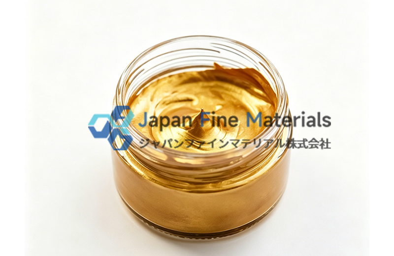
Gold Paste Materials and Structural Formation Mechanisms
The performance of gold paste stems from the synergistic interaction of multiple components, rather than relying solely on the metal content itself. A typical system generally comprises the following three core components:
1. Metal Phase
• High-purity gold powder (micron-scale / submicron-scale)
• A multi-particle-size blend system may be used
• Determines the conductive framework and the final dense structure
2. Organic carrier
• Solvent + resin + thickening system
• Controls printing rheological properties
• Determines pattern stability and drying behavior
3. Functional Additives
• Dispersants: Prevent agglomeration of gold particles
• Leveling agents: Improve print uniformity
• Sintering aids: Optimize the densification process
During the sintering process, the gold paste undergoes a typical three-stage structural evolution:
• Particle contact stage: Gold particles initially aggregate, forming a network of physical contacts
• Neck growth stage: Surface diffusion leads to strengthened interparticle connections
• Densification stage: Pores are reduced, forming a continuous metallic structure
The resulting structure more closely resembles a “sintered metal layer” rather than a simple aggregate of particles.
The Role of Thermal Management in Chip Bonding
The chip bonding layer serves as the primary heat transfer path in power semiconductor packaging. The role of gold paste in this structure is not merely to “secure the chip”; more importantly, it establishes a stable thermo-electric coupling interface. Its core functions are broken down as follows:
Establishment of a Thermal Conduction Path
• Formation of a low-porosity metal layer after sintering
• Improves the efficiency of heat transfer from the chip to the substrate
• Reduces localized heat buildup
Mechanical Bonding Stability
• Intermetallic diffusion forms a metallurgical bond interface
• More stable performance under thermal cycling conditions
• Reduced risk of interface fatigue
Control of structural uniformity
• Depends on the uniformity of the printed layer thickness
• Control of sintering shrinkage behavior
• Avoids localized stress concentration
Low-Loss Interconnects in RF Devices
In RF and microwave devices, a material’s “electromagnetic behavior” is more critical than its DC conductivity. The advantages of gold paste are primarily reflected in its ability to create low-loss interconnect structures.
Low-resistance signal paths
• Formation of continuous metal conductors after sintering
• Reduces contact resistance and transmission loss
Improved signal integrity
• Reduces impedance spikes
• Improves high-frequency transmission consistency
Reduces parasitic effects
• Reduce microgaps between particles
• Control local inductance variations
Electrode and Interface Behavior in Ceramic Packages
In ceramic packaging systems (Al₂O₃, AlN, etc.), gold paste is primarily used to form electrode layers or interconnect patterns, and the key challenge lies in “metal-ceramic interface matching.”
Electrode Pattern Formation
• Screen printing enables complex patterns
• Supports high-precision circuit design
• Used for constructing signal distribution structures
Interface Bonding Mechanism
• Relies on mechanical interlocking + surface wetting
• Forms a stable adhesion layer after sintering
• Highly sensitive to surface treatment
• The linear shrinkage rate of gold paste during sintering typically ranges from 5% to 12%
• Compensation must be factored into mask design
MEMS and Optoelectronic Packaging Applications
MEMS and optoelectronic devices place greater emphasis on “microscale control + low-stress stability” in material requirements.
Typical application scenarios:
• Electrode interconnections in microelectromechanical systems
• Local interconnections in optoelectronic chips
• Construction of heat sink connection paths
Key material performance requirements:
Low-stress characteristics
• Reduced risk of packaging deformation
• Prevention of displacement in sensitive structures
Locally Controlled Deposition
• Dispensing accuracy determines structural dimensions
• Supports micro-area functional design
Thermal stability
• Maintains long-term dimensional stability
• Reduces the impact of thermal drift
Conclusion
In semiconductor packaging, gold paste serves not only to provide electrical connections but also to facilitate heat conduction and support localized structural formation. In critical processes such as chip mounting, electrode formation, and high-frequency interconnects, its performance depends not only on the material itself but also heavily on overall process compatibility and structural design.
As packaging evolves toward higher integration density and greater reliability, the scope of gold paste applications continues to expand, and its role in complex packaging structures will become increasingly prominent.
For further information on gold paste application solutions and process compatibility assessments tailored to your specific packaging requirements, please contact JFM technical support team for consultation and available evaluation data.