How AuSn Solder Improves Semiconductor Packaging Reliability
-
2026-07-15 Industry News






Learn how AuSn solder improves semiconductor packaging reliability with strong thermal conductivity, stability, and hermetic sealing performance.
Introduction
Against the backdrop of high-reliability electronic devices continuously evolving toward higher power, higher frequencies, and miniaturization, the importance of packaging materials has been further amplified. Particularly in fields such as optical communications, power semiconductors, and high-frequency electronics, packaging serves not only as a protective structure but also directly determines the device’s thermal performance, electrical performance, and long-term stability.
AuSn solder has gradually been adopted in high-end semiconductor packaging due to its stable metallurgical properties and excellent overall performance, playing a crucial role in applications such as chip mounting and hermetic packaging.
What Is AuSn Solder?
AuSn solder typically refers to brazing materials in the gold-tin alloy system, the most common of which is the Au80Sn20 eutectic alloy.This alloy undergoes a eutectic reaction at approximately 278°C, transforming directly from the solid to the liquid state. The intermetallic compound phases formed upon solidification are primarily Au5Sn (ζ phase) and AuSn (δ phase), where Au5Sn is the primary phase and AuSn is the secondary phase in the eutectic mixture. Consequently, its microstructure differs from the “solid solution + eutectic structure” morphology of traditional tin-based solders.
In terms of material properties, the widespread adoption of AuSn Solder in high-end packaging applications is primarily due to the following key characteristics:
• High-melting-point system: With a eutectic point of approximately 280°C, it is suitable for high-temperature operating environments and subsequent secondary reflow processes
• Stable intermetallic compound structure: The microstructure remains stable after solidification and is not prone to significant diffusion-induced changes
• Excellent thermal stability: Maintains consistent performance even under prolonged high-temperature conditions
• Good mechanical strength and creep resistance: Suitable for applications involving frequent thermal cycling
• Low tendency for void formation: Contributes to improved packaging reliability
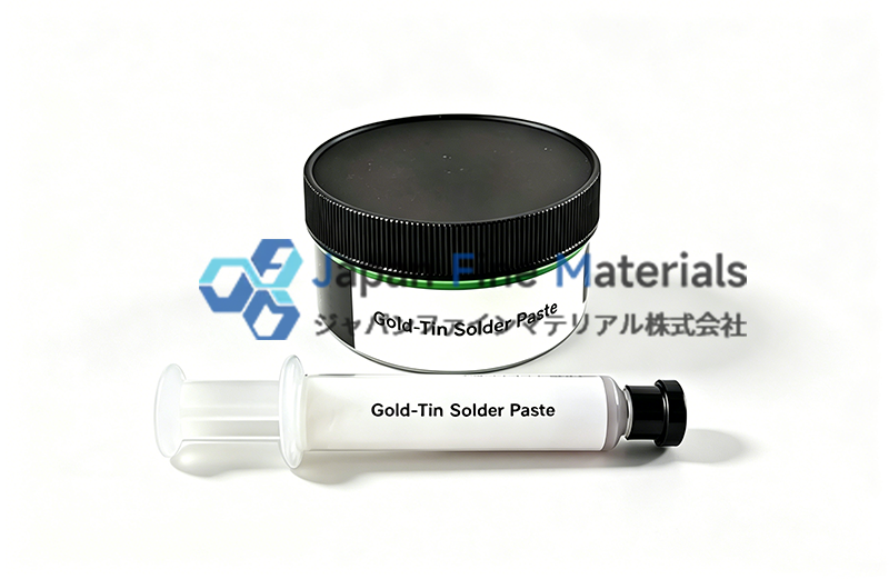
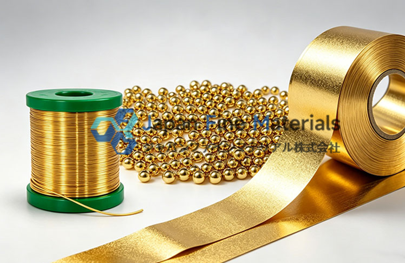
In practical engineering applications, AuSn solder is not typically used in its pure form but is processed into various forms according to packaging process requirements:
• Preformed solder pads: Used for high-precision chip mounting and planar connections
• Solder strips: Suitable for continuous soldering or structured soldering paths
• Solder paste: Suitable for complex structures or automated printing processes
Furthermore, because the AuSn system has low dependence on flux—and can even achieve flux-free soldering—it offers significant advantages in optoelectronics, RF devices, and hermetic semiconductor packaging. It effectively reduces the risk of residual contamination while improving packaging cleanliness and long-term stability.
Why Semiconductor Packaging Requires High-Reliability Materials
Semiconductor packaging serves as the critical interface between the device and the external environment; its role extends beyond mechanical fixation to include thermal management, electrical interconnection, and environmental isolation.
In practical applications, packaging materials typically face the following challenges:
• Prolonged operation in high-temperature environments
• Thermal cycling stress caused by high-frequency switching
• Mismatched coefficients of thermal expansion between different materials
• Stress concentration resulting from miniaturized structures
• Effects of high-humidity or corrosive environments
Under prolonged thermal cycling or high-temperature operating conditions, traditional solders are prone to interface fatigue, void propagation, or oxidation failure, which can compromise the overall device lifespan.
Therefore, in high-end applications, material systems often evolve toward higher melting points, greater stability, and lower diffusion rates. It is against this backdrop of demand that AuSn Solder has been widely adopted.
Key Advantages of AuSn Solder in Semiconductor Packaging
1. Excellent Thermal Conductivity
AuSn alloys have high thermal conductivity, effectively reducing the thermal resistance between the chip and the substrate in power devices and optoelectronic devices.
In applications such as lasers, RF modules, and power MOSFETs (metal-oxide-semiconductor field-effect transistors), failure to rapidly dissipate heat can directly lead to degraded device performance or even failure. AuSn solder helps establish a stable thermal conduction path, thereby improving overall thermal performance when properly designed.
2. Excellent Mechanical Reliability
Due to the stability of its intermetallic compound structure, AuSn solder joints exhibit low creep rates and strong fatigue resistance under thermal cycling conditions.
This stability is particularly critical in long-term service scenarios such as aerospace or automotive electronics. Compared to low-melting-point solder systems (such as SnPb or SAC), AuSn Solder exhibits lower rates of microstructural coarsening and intermetallic compound growth in high-temperature environments.
3. Excellent hermetic sealing performance
In optical communication modules, MEMS devices, and certain sensors, hermetic sealing is a critical factor in ensuring device longevity.
After solidification, AuSn solder has a dense structure and low porosity; when combined with appropriate soldering processes and interface designs, it can effectively reduce the pathways for water vapor and oxygen permeation, thereby enhancing the reliability of hermetic sealing.
Therefore, it is one of the most commonly used sealing materials in packages and optoelectronic module packaging.
4. Supports Flux-Free Processes
AuSn solder exhibits good wettability toward gold or nickel plating layers above the eutectic temperature, typically enabling flux-free soldering.
This is particularly important for packaging applications with high cleanliness requirements, as flux residues may lead to:
• Ionic contamination
• Electrical performance drift
• Reduced long-term reliability
In optoelectronic and high-frequency devices, the no-flux process can significantly improve packaging consistency and long-term stability.
Typical Applications of AuSn Solder in Semiconductor Packaging
AuSn solder is primarily used in packaging structures with high requirements for reliability and thermal performance:
|
Application Areas |
Typical Devices |
|
Optical Communications |
Laser diodes, optical transceiver modules |
|
Power Semiconductors |
MEMS (Micro-Electro-Mechanical Systems) Sensors and Actuators |
|
RF/Microwave Devices |
RF amplifiers, microwave packaged modules |
|
MEMS |
Sensors and MEMS Structures |
|
Medical Electronics |
Highly Reliable Implantable or Monitoring Devices |
These applications share the following characteristics: extremely low tolerance for failure and complex operating environments.
AuSn Solder vs. Traditional Solder
From an engineering perspective, the differences between various solder systems essentially stem from differing design objectives: traditional solders emphasize process compatibility, while AuSn solders prioritize high reliability and stability under extreme operating conditions.
1. Melting Point and Operating Temperature Window
Traditional Solder (SnPb / SAC)
• Low melting point (approximately 183°C–217°C)
• Suitable for medium- and low-temperature electronic assembly
• Wide process window, making it easy to mass-produce
AuSn Solder
• Eutectic melting point of approximately 280°C
• Suitable for high-temperature packaging processes
• Better suited for high-power and high-temperature operating conditions
AuSn is a material system more suited for high-temperature applications and is not suitable as a replacement for general-purpose consumer electronics.
2. Long-Term Reliability and Microstructural Stability
Traditional solder
• Intermetallic compounds continue to grow under long-term thermal cycling
• Prone to embrittlement or interfacial fatigue
• Significant performance degradation in high-temperature environments
AuSn Solder
• Forms a stable intermetallic compound structure (AuSn system)
• Low creep rate
• Greater thermal cycling stability
AuSn offers clear advantages in long-life, high-reliability applications.
3. Thermal Conductivity and Thermal Management Capabilities
Traditional Solder
• Moderate thermal conductivity
• Performance degrades with aging
• High sensitivity to voids
AuSn Solder
• High thermal conductivity
• Good interfacial stability, minimal change in thermal resistance
• Better suited for high-power-density chips
AuSn is better suited for applications with sustained high heat flux density.
4. Process Dependency and Assembly Difficulty
Traditional Solder
• Can use flux
• High process tolerance
• Suitable for large-scale automated production
AuSn Solder
• Flux-free process in most cases
• High surface cleanliness requirements
• Requires stricter temperature profile control
The AuSn process has a higher learning curve but offers superior consistency.
AuSn is not an upgraded version of traditional solder, but rather a distinct category of structural materials designed for high-end semiconductor packaging systems.
Guidelines for Selecting AuSn Solder
Selecting AuSn solder requires a comprehensive consideration of packaging structure, thermal design, and process capabilities—it is not simply a matter of material substitution. Different application scenarios place varying emphasis on solder form and performance, so decisions are typically made based on several key dimensions.
1. Packaging Structure and Size Compatibility
For small-sized, high-precision chip mounting (such as lasers or RF devices), AuSn preformed solder sheets are preferred to ensure thickness uniformity and interface consistency; whereas in scenarios with complex structures or requiring localized wetting, solder paste or solder tape may be more suitable.
2. Thermal Management Requirements
When device power density is high, priority must be given to the continuity of the solder’s thermal path and the control of interfacial thermal resistance; in such cases, uniform material spread and void rate control become particularly critical.
3. Packaging Reliability Grade Requirements
For aerospace or long-life industrial applications, the more stable eutectic Au80Sn20 system is typically preferred to ensure that the structure does not undergo significant degradation under long-term thermal cycling.
4. Process Compatibility
This includes the capabilities of reflow equipment, support for vacuum environments, and substrate plating systems (such as Au/Ni/Au structures). These factors often directly determine whether the solder can wet the substrate stably and whether interfacial defects are likely to occur.
Overall, selecting an AuSn solder ——is more of a “systems engineering decision” than a comparison of individual material parameters; it requires striking a balance among performance, structure, and process.
Conclusion
In high-reliability semiconductor packaging systems, material selection often determines the upper limit of device performance. Thanks to its excellent thermal stability, mechanical reliability, and hermeticity, AuSn solder has become one of the key bonding materials in the fields of optoelectronics, power devices, and high-end packaging.
For electronic systems requiring long-term stable operation in harsh environments, the appropriate selection of AuSn solder materials directly impacts product reliability and service life.
If you are selecting materials for a related packaging project or need to evaluate ’s AuSn solder solutions for specific applications (such as lasers, power modules, or hermetic packaging), please contact us for further technical support and material recommendations.
JFM offers AuSn preformed solder pads, solder ribbons, and solder paste in a variety of specifications, and supports the development of customized solutions tailored to specific packaging structures and reliability requirements.