BGA Solder Ball Guide for Semiconductor Packaging
-
2026-07-22 Industry News






This article introduces BGA solder balls in semiconductor packaging and their role in ensuring stable chip connections, improving device reliability, and enabling compact electronic designs.
Introduction
As semiconductor devices continue to evolve toward miniaturization, high performance, and high integration, the importance of packaging technology is growing. Whether it’s processors in smartphones, memory chips in servers, or control modules in automotive electronics, packaging quality directly impacts product performance and reliability.
Among the many packaging materials, BGA solder balls—though minuscule in size— serve as a vital medium for connecting chips to external circuits. For semiconductor packaging companies, EMS providers, and electronics manufacturers, understanding the material properties, specification selection, and quality requirements of BGA solder balls is fundamental to ensuring packaging yield and product reliability.
What Are BGA Solder Balls?
A BGA solder ball is a preformed spherical solder ball primarily used in semiconductor packaging and high-density electronic assembly. Depending on packaging requirements, its diameter typically ranges from 0.1 mm to. Some advanced packaging applications (such as fine-pitch WLCSP) may use specifications ranging from 0.15 mm to 0.25 mm;In 3D integration and chip stacking, micro-bumps can be further reduced to approximately 0.05 mm, though their manufacturing process from that of BGA 0.76 mmdiffers BGA solder balls.
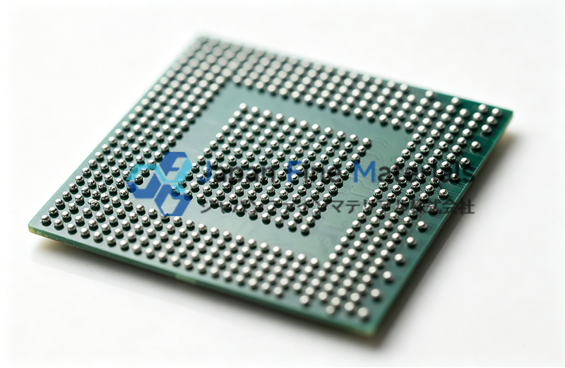
As electronic products evolve toward thinner, lighter designs and higher integration, chips need to accommodate more connection points within a smaller space. Traditional wire-bonded packaging is increasingly unable to meet these demands, whereas array-based BGA solder balls can provide higher I/O density within a limited area and are therefore widely used in packaging technologies such as BGA, CSP, WLCSP, and flip-chip.
BGA solder balls feature the following characteristics:
• A wide range of sizes to meet various packaging design requirements
• High sphericity, facilitating automated ball placement and assembly
• Alloy composition can be adjusted according to specific application scenarios
• Suitable for high-density, high-reliability electronic packaging
• Supports lead-free and special alloy system requirements
Currently, BGA solder balls have become one of the essential base materials in the packaging processes for products such as smartphone chips, memory devices, communication modules, automotive electronics, and industrial controllers.
The Primary Role of BGA Solder Balls in Semiconductor Packaging
Although BGA solder balls are minuscule in size, they perform multiple critical functions in semiconductor packaging. From electrical connections to mechanical support and reliability assurance, their performance directly impacts packaging quality and the stability of the final product.
1. Establishing a Stable Electrical Connection
The most fundamental and crucial role of BGA solder balls is to establish a reliable electrical connection between the chip package and the PCB.
During the reflow soldering process, BGA solder balls melt and form solder joints, enabling power, control signals, and data signals from within the chip to be transmitted smoothly throughout the electronic system. Compared to traditional leaded packages, the BGA array structure provides a higher number of I/O pins while shortening signal transmission paths, which helps improve high-speed signal transmission performance.
2. Providing Mechanical Support
In addition to their electrical conductivity, BGA solder balls also play a crucial role in supporting the package structure.
Once the chip is mounted on the PCB, the solder joints must withstand vibrations, impacts, and external stresses generated during transportation, assembly, and actual use. A stable solder joint structure helps the package maintain good mechanical strength and reduces the risk of connection failure caused by external forces.
3. Mitigating the Effects of Thermal Stress
Semiconductor devices continuously undergo heating and cooling cycles during operation, and the coefficients of thermal expansion for the chip, package substrate, and PCB differ.
This discrepancy generates sustained thermal stress in the connection area. BGA solder balls can absorb and dissipate some of this stress through their material properties, thereby reducing the risk of solder joint fatigue cracking and breakage, and improving the product’s long-term operational reliability.
4. Support for High-Density Packaging Designs
As electronic products continue to evolve toward miniaturization and higher performance, packaging structures must accommodate more connection points within limited space.
The BGA solder ball array design effectively increases I/O density, meeting the high-integration requirements of advanced packaging. Currently widely used in packaging technologies such as BGA, CSP, WLCSP, and SiP, it serves as one of the key foundations for achieving high-density packaging.
Types of BGA Solder Ball Materials
Sn63Pb37 (Tin-Lead Alloy)
This is a solder system widely used in traditional electronic packaging, with the following characteristics:
• Low melting point
• Good wetting properties
• Mature process technology
• Wide soldering window
However, due to environmental regulations, its scope of application is gradually decreasing.
SAC305 (Sn96.5/Ag3.0/Cu0.5)
This is one of the more widely used lead-free solders, with key advantages including:
• Compliance with RoHS requirements
• Good mechanical strength
• High thermal cycling reliability
• Widely used in consumer electronics and industrial electronics
Special alloy systems
For automotive electronics, high-reliability industrial equipment, or special packaging requirements, some manufacturers use customized solder systems, such as:
• Low-silver solder
• High-reliability lead-free solder
• Low-temperature solder
• Micro-alloyed solders
These materials are typically used to optimize reliability under specific operating conditions.
How to Select the Appropriate BGA Solder Ball Specifications?
Selecting the right BGA solder ball specifications is not simply a matter of choosing a size; rather, it is a systematic decision that requires balancing package structure, process capabilities, and end-use reliability requirements.
1. Determine the basic range based on package type and structural design
Different package structures impose vastly different constraints on BGA solder ball specifications:
• Standard BGA packages: Relatively ample space, allowing for a wide range of ball diameters
• CSP / WLCSP packages: Space is extremely limited, requiring smaller ball diameters and higher consistency
• System-in-Package (SiP): Typically involves a mix of various devices and is more sensitive to pitch and coplanarity
• Flip-chip-related structures: Tend toward micro-pitch designs and require extremely tight dimensional tolerances for BGA solder balls
Generally speaking, the smaller the package size and the higher the I/O density, the more BGA solder ball specifications tend toward miniaturization and higher precision.
2. Calculating Ball Diameter Based on BGA Solder Ball Pitch
Pitch is one of the core parameters determining the specifications of BGA solder balls, and there is a direct relationship between the two. In engineering practice, a fundamental principle is typically followed: the ball diameter must maximize the effective soldering area while ensuring a safe margin for pitch.
If the ball diameter is too large:
• Bridge formation is likely to occur
• Increased risk of reflow collapse
• Poorer coplanarity control
If the ball diameter is too small:
• Insufficient solder joint contact area
• Reduced mechanical strength
• Reduced reliability (especially thermal cycle life)
However, in fine-pitch designs, a reduction in ball diameter is typically accompanied by a reduction in pad size, which correspondingly decreases the thermal cycle life of the solder joint Reliability must be compensated for through structural or material measures—such as underfill or low-α solderrather than simply increasing the ball diameter.—.
Therefore, during the design phase, it is essential to perform a comprehensive match that takes into account PCB pad size, solder mask openings, and pad spacing, rather than selecting components in isolation.
3. Adjustment Based on I/O Count and Current Load Requirements
BGA solder balls not only facilitate signal connections but may also carry a certain amount of current. Special attention must be paid to specification matching in the following situations:
• High-I/O-density chips (SoC / GPU / FPGA)
• Packages with a large number of power pins
• High-power modules (e.g., RF power amplifiers, automotive ECUs)
Generally speaking:
• Larger ball diameter: lower resistance, higher current-carrying capacity
• Smaller ball diameter: Higher density, smaller footprint
• Therefore, a balance must be struck between electrical performance and space constraints.
4. Match the PCB pad design with process capabilities
Even with a well-designed package, problems may still arise if it is not compatible with the PCB’s capabilities. Key considerations include:
• Pad size
• Solder mask design
• Coplanarity control capabilities
• Reflow soldering temperature profile capabilities
• Support for a nitrogen-based reflow environment
For example, on high-density PCBs, if the solder mask openings are too small or misaligned, this will directly affect the wetting and formation quality of BGA solder balls.
5. Select Material and Specification Combinations Based on Application Reliability Levels
Reliability requirements for BGA solder balls vary significantly across different application scenarios:
• Consumer electronics: Prioritize cost and yield
• Industrial electronics: Emphasis on stability and service life
• Automotive electronics: Emphasis on thermal cycling, vibration, and adaptability to extreme environments
• High-reliability communications equipment: Emphasis on long-term stability and low failure rates
In high-reliability applications, it is typically necessary not only to select the appropriate ball diameter but also to use:
• Lead-free systems such as SAC305 and SAC405
• Stricter sphericity control
• Materials with lower oxidation levels
Key Factors Affecting the Quality of BGA Solder Balls
Dimensional Consistency
Excessive dimensional deviations in BGA solder balls may result in:
• Difficulty in ball placement
• Insufficient coplanarity
• Inconsistent solder joint height
• Increased reflow soldering defects
High-precision ball diameter control is a key prerequisite for ensuring packaging yield.
Sphericity
Ideally, BGA solder balls should maintain a high degree of sphericity. Insufficient sphericity may affect:
• Automatic ball placement efficiency
• Solder joint formation quality
• Soldering consistency
This is particularly important for fine-pitch packages.
Surface Oxidation Control
Solder materials are highly sensitive to oxidation, especially in lead-free systems. BGA Solder Ball Surface oxidation reduces wetting performance; in severe cases, the following may occur:
• Cold solder joints
• Poor wetting
• Interface embrittlement of solder joints
• Incomplete reflow fusion
Therefore, oxidation levels must be strictly controlled during production, packaging, and storage.
Alloy Composition Stability
The core quality of BGA solder balls depends primarily on the alloy system itself, such as SnAgCu (SAC) or tin-lead systems. Even minor fluctuations in composition can affect:
• Melting point shift
• Changes in wetting behavior
• Inconsistent joint strength
• Reduced thermal fatigue life
Therefore, stable metallurgical control is one of the key criteria for manufacturing high-quality BGA solder balls.
Conclusion
For the semiconductor packaging industry, although BGA solder balls are only a tiny component in the entire packaging structure, they are directly related to packaging quality, production yield, and product reliability.
From material selection to specification matching, and from dimensional control to reliability verification, every step requires strict control. Only by selecting BGA solder balls that meet application requirements can a stable foundation be provided for subsequent packaging manufacturing and the ever-increasing market demands be met.
Contact JFM for Professional Support
If you are looking for high-quality BGA solder ball products, or if you need specification selection and technical support for your semiconductor packaging projects, please contact JFM. We can provide professional solutions tailored to different packaging formats and application scenarios to help you improve packaging reliability and production efficiency.