The Role of BGA Solder Ball in CSP Packaging
-
2026-07-22 Industry News






This article reviews the role of BGA solder balls in CSP packaging, focusing on interconnection reliability and device miniaturization.
Introduction
In advanced semiconductor packaging systems, CSP (chip-scale packaging) has become one of the mainstream solutions for high-density integrated circuits. Its core objective is to achieve higher I/O density and superior signal transmission performance within a package size close to that of the chip itself, thereby meeting the demands of miniaturization and high-speed applications.
As packaging structures have evolved from traditional lead-based designs to array-based interconnects, BGA solder balls have become a critical component in CSP packaging. They establish the electrical connection between the chip and the substrate and play a role in distributing mechanical and thermal stresses across the overall structure.
In practical applications, solder balls not only affect electrical continuity but are also closely related to the package’s reliability under thermal cycling conditions. Therefore, they serve as core interconnection elements within the CSP structure that simultaneously influence both electrical performance and mechanical reliability.
Interconnection Path Logic in CSP Packaging
Structurally, the core feature of CSP packaging is routing the chip’s electrical signals through shorter, more direct paths, thereby enhancing performance and reducing signal loss.
In actual packaging, signal transmission typically follows the following path:
• Chip pads
• UBM metal layer
• RDL (Re-wiring Layer)
• BGA solder ball
• PCB pad
Compared to traditional wire bonding methods, the most significant change in this structure is the shift from linear wire connections to vertical array interconnects.
The function of each layer is also clearly defined:
• UBM Layer: Provides a weldable metal interface between the chip’s aluminum pads and the solder, prevents harmful diffusion between the aluminum and the solder, and ensures metallurgical stability at the interface
• RDL Layer: Responsible for redistributing the fine-pitch pads on the chip into a layout more suitable for packaging
• BGA Solder Balls: Provide the final electrical connection and mechanical attachment between the package and the PCB
Because signal paths are significantly shortened, CSP packaging can effectively reduce parasitic inductance and signal delay, which is critical for high-speed signal transmission (such as in memory chips and communication chips).
Furthermore, the array-based interconnect combined with underfill technology effectively dissipates thermomechanical ,,stress. Compared to traditional wire bonding, CSP offers significantly improved reliability under thermal cycling and mechanical shock.
The Three Major Roles of BGA Solder Balls in CSP Packaging
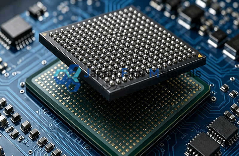
In the CSP packaging structure, the BGA solder ball serves not merely as a connection point, but as a multifunctional interface layer that simultaneously addresses electrical, mechanical, and structural design constraints.
Occupying a critical intermediate layer within the packaging system, it amplifies overall performance; despite its small size, it has a direct impact on failure modes and reliability limits.
1. Electrical Interconnection: Low-Impedance Signal Transmission Path
In the CSP structure, BGA solder balls serve as the final electrical connection path between the chip and the PCB; their performance depends not only on electrical conductivity but also on the stability of the interfacial metallurgical structure.
Key engineering considerations include:
• Interconnection resistance or solder joint resistance
• IMC layer thickness control (Cu6Sn5 / Cu3Sn)
• Solder joint uniformity
In high-speed signal applications (such as 5G RF or high-speed memory), solder ball geometry directly affects:
• Impedance matching
• Signal reflection
• Crosstalk
2. Mechanical Buffering: Structures for Releasing Thermal Expansion Mismatch
CSP packages typically present CTE (coefficient of thermal expansion) mismatch issues:
• Silicon chip: ≈ 2.6 ppm/°C
• PCB substrate: ≈ 14–17 ppm/°C
This difference generates shear stress during thermal cycling.
BGA solder balls absorb these stresses through the creep and plastic deformation of the solder alloy. During thermal cycling, their mechanical response typically manifests as follows:
• Low-stress/low-temperature phase: Primarily elastic deformation
• Moderate-stress/high-temperature phase: Creep deformation (stress relaxation)
• High-stress/high-strain-rate phase: Plastic deformation
Their reliability depends on the creep fatigue life of the solder.
3. Package Density Control: Coupled Design of Pitch and Ball Diameter
The essence of CSP packaging is the reorganization of I/O within a limited space, and the BGA Solder Ball array defines the geometric boundary conditions of this structure.
At the design level, the Solder Ball directly constrains the following parameters:
• Array pitch
• Ball diameter
• Pad aperture size
There is a strong coupling between these three factors:
• The smaller the pitch: the higher the requirement for ball diameter consistency
• Ball diameter deviation: directly affects the risk of bridging
• High-density arrays: Extremely sensitive to ball roundness
In designs with pitch sizes below 0.4 mm, the dimensional tolerances for Solder Balls typically need to be controlled at the micrometer level.
Key Process Chain for Solder Balls in CSP Packaging
The final performance of BGA solder balls in CSP packaging depends not only on the material itself but also on the quality control of the entire packaging process. Generally, the quality of the solder joints is determined by several key steps working in concert.
1. UBM Layer Preparation (Pad Interface Treatment)
Before ball placement, a transition metal layer (UBM) must be formed on the chip pads. Its primary functions are:
• Improve solder adhesion
• Preventing failure caused by metal diffusion
• Control the solder joint interface reaction
If this layer is not properly prepared, even if the Solder Ball itself meets quality standards, de-soldering or interface instability may occur.
2. Solder Ball Placement
This step involves placing the solder balls in an array onto the corresponding pad positions. Key control points include:
• Whether the solder balls are properly aligned
• Whether the ball diameters are consistent
• Whether there are any misalignments or missing balls
In high-density CSP structures, the precision of this step is critical, as even minor deviations can be magnified during the subsequent reflow process.
3. Reflow Soldering
Reflow soldering is the process by which the solder balls at are truly formed and bonded.
As the temperature rises:
• The solder ball melts
• It wets the pad
• and, upon cooling, form a stable solder joint
The main factors affecting the solder joint during this stage are:
• Bond strength
• Uniformity of internal structure
• Long-term reliability
If the temperature profile is not properly controlled, problems such as cold joints, internal voids, or weak connections are likely to occur.
4. Cleaning and Residue Control
Flux residues typically remain after reflow; if not thoroughly removed, they may pose long-term risks, such as:
• Corrosion
• Deterioration of insulation properties
• Increased risk of electromigration
Therefore, for high-reliability products, cleaning is generally performed or low-residue materials are used.
5. Inspection and Quality Verification
Finally, the solder joints must be inspected. Common methods include:
• X-ray inspection of internal structure
• Visual inspection for misalignment or missing joints
• Reliability testing (e.g., thermal cycling)
The purpose is to verify that the solder joints meet requirements in terms of both structure and reliability.
Analysis of Typical Failure Modes
In CSP packages, BGA solder balls are typically subjected to high stress, high current density, and complex thermal cycling environments. Their failure is not due to a single cause but rather the combined result of materials, structure, and process factors. Common engineering issues can be categorized into four types: voids, fatigue fracture, interface degradation, and electromigration.
1. Solder Joint Voids
Solder joint voids primarily result from gases failing to escape in a timely manner during the reflow process, which are then trapped as the solder solidifies, forming cavities.
Common causes:
• Insufficient venting of flux volatiles
• Inappropriate reflow temperature profile (insufficient heating or hold time)
• Oxidation of the pads, leading to poor wetting
• Contamination on the solder ball or pad surface
Engineering Implications:
• Reduced effective contact area
• Increased local current density
• Decreased thermal conductivity
• Prone to localized overheating in high-power scenarios
2. Thermal Cycle Fatigue Fracture
Due to the significant CTE difference between the chip and the PCB, solder balls are subjected to continuous shear stress during thermal cycling.
Failure mechanism:
• Microcracks initiate at the edges of the solder joints
• Cracks propagate along grain boundaries or IMC layers
• The cross-section of the solder joint gradually weakens
• Ultimately, an open-circuit failure occurs
High-Risk Areas:
• Corner solder balls of the BGA package
• Locations far from the neutral point
3. Interface Failure and Abnormal IMC Growth
Intermetallic compounds (IMCs) form between the solder ball and the copper pad; while these are critical to the strength of the connection, they also represent a point of weakness.
Main Issues:
• Excessive growth of the IMC layer leads to increased brittleness
• Thermal aging causes interfacial delamination
• Uneven diffusion results in localized weak bonding
Engineering Consequences:
• Decreased shear strength
• Reduced drop resistance
• Greater susceptibility to failure under mechanical shock
4. Electromigration Failure
Under high current density conditions, metal atoms undergo directed migration driven by the flow of electrons.
Manifestation:
• Voids form in the cathode region
• Material buildup in the anode region
• Increased local resistance or even an open circuit
Factors Affecting This Phenomenon:
• Current density
• Operating temperature
• Degree of solder joint miniaturization
• Stability of the alloy system
Engineering Applications
The application of BGA solder balls in CSP packaging serves as a critical interconnect material for high-density, high-frequency, and high-reliability system-on-chip (SoC) packaging. Consequently, their application scenarios typically focus on fields with extremely stringent requirements for size, signal integrity, and long-term stability.
1. Smart Devices and Mobile Computing Chips
Main Applications:
• Mobile Phone SoC Chips
• Memory chips
• RF modules
CSP packaging is widely used in smartphones and consumer electronics. The core driving force behind this trend is the continuous evolution of products toward thinner, lighter, and higher-performance designs, which places greater demands on packaging space and integration density.
In this field, BGA solder balls are primarily used to achieve high-density interconnects while ensuring the stability of high-speed signal transmission, which directly impacts overall power consumption and performance.
2. High-Speed Memory and Data Processing Devices
Main Applications:
• DRAM
• NAND Flash
• SSD Controller Chips
These products typically operate under high-speed data read/write conditions and place high demands on the stability of package interconnects. Even slight degradation in signal integrity can affect the accuracy of data read/write operations, particularly in high-speed interfaces.
The primary role of solder balls here is to ensure the reliability of high-speed signal transmission while reducing resistance and signal loss, thereby enhancing long-term operational stability.
3. Automotive Electronic Control Systems
Main Applications:
• ECU (Engine Control Unit)
• ADAS Systems
• Battery Management Systems
Automotive electronics are typical high-reliability applications that require long-term, stable operation in complex environments, placing higher demands on packaging materials.
Its key characteristics are a wide temperature range (-40°C to 150°C) and exposure to high-vibration environments; therefore, BGA solder balls must possess excellent thermal fatigue resistance and structural stability to prevent cracking or failure during long-term use.
4. Communications and High-Frequency RF Modules
Main Applications:
• 5G base stations
• RF front-end modules
• Communications chips
Communication equipment is highly sensitive to signal quality, especially in high-frequency environments, where packaging defects (such as solder ball misalignment or voids) are more likely to cause a decline in signal integrity.
The core function of solder balls here is to maintain a stable signal path, reduce transmission loss, and enhance the overall reliability of electrical connections.
5. Industrial Control and Embedded Systems
Main Applications:
• PLC Controllers
• Industrial robot control boards
• Embedded Systems
Industrial control equipment typically requires long-term continuous operation and demands high levels of stability and reliability, especially in complex industrial environments.
In this field, BGA solder balls are primarily evaluated for their long-term reliability, including oxidation resistance, low failure rates, and stability during continuous operation.
Conclusion
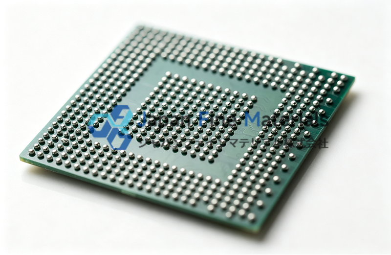
In the CSP packaging system, the role of BGA solder balls can be summarized as follows:
• Structural Connection Unit
• Stress-absorbing medium
• Reliability Control Node
It is not merely a simple bonding material, but rather a key structural unit that simultaneously provides electrical interconnection, mechanical stress relief, and overall package reliability control. From an engineering perspective, it directly influences signal transmission quality, thermal cycling life, and long-term operational stability; its performance depends on the synergistic optimization of multiple factors, including the material system, solder ball diameter consistency, and reflow soldering process control.
Therefore, BGA Solder Balls are, by their very nature, a core component of package performance, rather than a standalone consumable.
If you require specification matching, alloy selection, or reliability optimization solutions for BGA Solder Balls tailored to different CSP package grades, please contact JFM at technical for support and customized solutions.