Key Precious Metals Used in Semiconductors Manufacturing
-
2026-07-22 Industry News






Overview of how key precious metals are applied in semiconductor manufacturing, including interconnects, electrodes, and thin-film processes.
Introduction
In the semiconductor manufacturing system, materials are not merely functional carriers; they directly influence the electrical performance, thermal stability, and long-term reliability of devices. Particularly against the backdrop of continuous advancements in advanced processes and high-density packaging, Precious Metals have gradually evolved from “auxiliary materials” to become integral components of critical functional layers.
From front-end wafer processes to packaging interconnect structures, and on to thin-film deposition and sensor applications, different Precious Metals play distinct roles within their respective process windows. Understanding the rationale behind the application of these materials facilitates more rational process design and material selection.
Package Interconnect System
The packaging interconnect layer serves as the primary interface between the chip and external systems; its core function is to maintain a stable connection under the combined effects of thermal cycling, mechanical stress, and current density.
Precious Metals in this system primarily exist in the form of solder alloys, solder ball structures, and interface metal layers. Their selection is typically driven by the following factors:
• Thermal expansion coefficient matching
• Ability to control void rates
• Resistance to electromigration
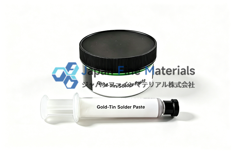
1. High-Reliability Packaging Solder (Au–Sn System)
The Au–Sn eutectic system is widely used in high-reliability packaging and is particularly suitable for:
• Hermetic packaging
• RF and microwave devices
• Aerospace and defense electronic systems
Its key advantages include:
• A well-defined eutectic point (278°C) and stable solidification behavior
• Forms an intermetallic compound (IMC) layer, making it resistant to creep under long-term high-temperature conditions
• Strong oxidation resistance, suitable for sealed environments
However, its limitations include high cost and strict requirements for interface cleanliness.
2. Sn–Ag–Cu (SAC) Solder System
In consumer electronics and standardized packaging, the SAC system (such as SAC305) remains the mainstream choice.
By incorporating Ag and Cu:
• Improved wettability and mechanical strength
• Improved thermal cycling life
• Optimizes current-carrying capacity
Its performance primarily depends on the β-Sn grain structure and the distribution pattern of the Ag₃Sn precipitate phase.
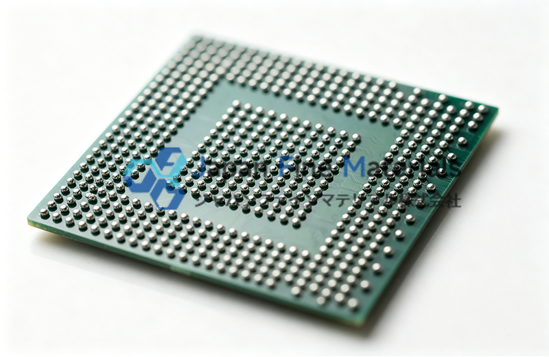
3. Solder Ball Interconnect Structures (BGA / Flip-Chip)
In high-density packaging, solder balls serve as the array interconnects between the chip and the substrate. Key areas of development include:
• Miniaturization
• Void Suppression
• Copper-core solder balls
In BGA packaging, the introduction of copper-core solder balls reduces resistance and increases current-carrying capacity while maintaining spherical interconnects; in flip-chip packaging, copper pillar bumps enable higher-density chip-level interconnects through an electroplated copper pillar structure.
Chip Bonding Systems
Bonding systems directly affect the resistance distribution, signal delay, and long-term drift characteristics of internal chip interconnects, making them a key constraint in high-frequency device design.
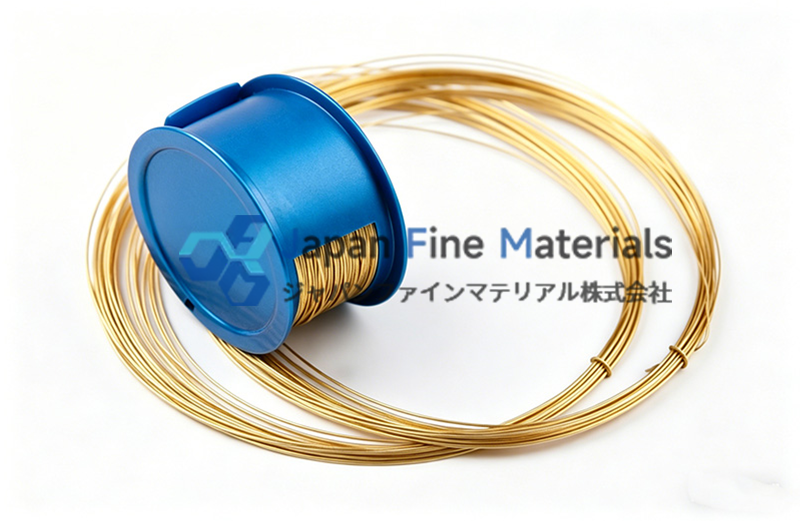
1. Gold Bond Wire Systems
Gold bonding wires are still widely used in high-reliability devices, and their advantages are primarily reflected in:
• High chemical inertness and excellent corrosion resistance
• Stable electrical conductivity (low signal drift)
• Wide bonding window
In high-end applications, the following are also used:
• Au–Pd alloy wires (to improve resistance to bending fatigue)
• Au–Cu systems (to reduce material costs and optimize mechanical strength)
The bonding mechanism typically involves thermo-ultrasonic bonding, which relies on the combined effects of interfacial diffusion and plastic deformation.
2. Eutectic and Intermetallic Compound Bonding Systems
The Au–Sn eutectic system is used for high-reliability hermetic packaging; the Au–Ge eutectic system is primarily used for die attach on the backside of compound semiconductor (e.g., GaAs) chips. Its key features are:
• Formation of a metallurgical bond interface via intermetallic compounds (IMCs)
• Maintaining structural stability under high-temperature conditions
• Suitable for packaging high-power-density devices
3. Evaporation and Thin-Film Precursor Systems
In some advanced devices, gold and its alloys are used for:
• Electron beam evaporation
• Thermal evaporation
Forming nanoscale metal films for:
• Ohmic contact layers
• Gate structures
• Reflective layers or barrier layers
Semiconductor test systems
The testing phase is essentially a “high-frequency micro-contact system”; the materials must not only be electrically conductive but also maintain interface stability under high-frequency repeated contact.
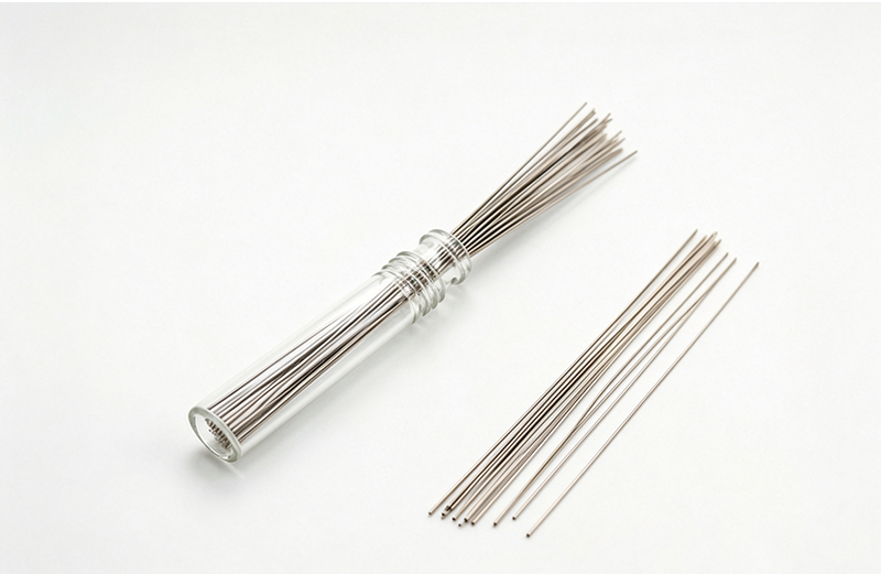
1. Probe System Materials
Mainly include:
• Tungsten-based probes (W alloy)
• Beryllium copper probes (BeCu)
• Palladium-alloy-plated probes
Key Performance Indicators:
• Contact resistance stability
• Mating Cycle Life
• Resistance to Contamination
2. High-Current Test Structure
Designed for power device testing, with a focus on:
• Low-inductance path design
• Spring contact stability
• precious metals -plated (Au / PdNi)
3. Materials Engineering Rationale
The introduction of palladium- and platinum-based materials is primarily intended to reduce oxide film formation and micro-weld wear.
Thin-Film Deposition Systems
In advanced manufacturing processes, Precious Metals targets are used in PVD and sputtering processes to form nanoscale thin-film structures, which serve as one of the foundational layers for device functionality.
1. Precious Metals Target System
• Au (High-Conductivity Electrode Layer)
• Pt (Stabilizing Electrode/Catalytic Layer)
• Ru (barrier layer/capacitive electrode)
Key Specifications:
• Purity (≥99.99%)
• Grain uniformity
• Sputtering rate stability
2. Thin-Film Formation Mechanism
During the sputtering process:
• Plasma Bombardment of Target Materials
• Atomic-level particle deposition on the wafer surface
• Formation of continuous or multilayer nanostructures
This process has a significant impact on the film’s resistivity, interfacial adhesion, and long-term thermal stability.
Conductive Functional Material Systems
This system is primarily used for “non-wafer-level interconnects” and plays a role in packaging and module-level structures.
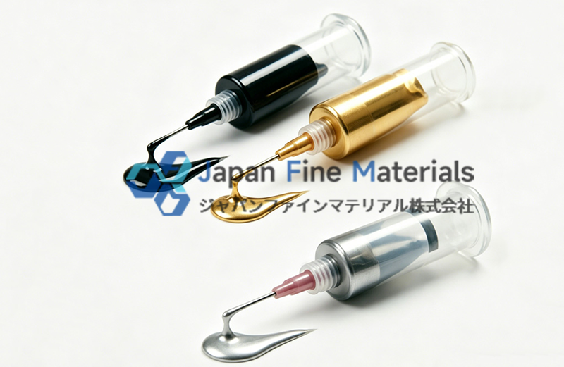
1. Metal paste systems
Includes:
• Gold paste
• Silver paste
• Platinum paste
Main Applications:
• Thick-film circuits
• Chip mounting
• Formation of conductive paths
Its core performance depends on:
• Sintering density
• Particle size distribution
• Volatilization behavior of the organic binder
2. Conductive Adhesive Systems (ICA / ACA)
• ICA: Isotropic Conductive Adhesive (uniform conductivity)
• ACA: Anisotropic conductive adhesive (Z-axis conductivity)
Key Control Points:
• Filler Dispersion
• Probability of contact between conductive particles
• Curing Shrinkage Stress
3. Silver Nanoparticle Sintering Systems
Applications in power semiconductors (SiC/GaN) are growing rapidly, with advantages including:
• High thermal conductivity (typically 150–250 W/m·K, depending on sintering density and porosity)
• High-melting-point bonding (solid-state sintering)
• Excellent current density carrying capacity
Essentially a “high-temperature alternative” to traditional solder systems.
Precious Metals Materials Used in Semiconductors
From a materials perspective, the Precious Metals and related functional materials currently used in the semiconductor industry primarily include the following categories:
|
Material Category |
Typical Materials |
Typical Application Stages |
|
Gold (Au) System |
Au, AuSn, AuGe, AuPd |
Bond wires, eutectic solders, thin-film electrodes |
|
Silver (Ag) System |
Ag, nanosilver, Ag paste |
Sintered connections, conductive pastes, packaging interconnects |
|
Platinum (Pt) System |
Pt, Pt alloys, Pt paste |
Thin-film electrodes, sensor structures |
|
Palladium (Pd) System |
Pd, Pd-Ni alloys |
Probe coatings, contact materials |
|
Ruthenium (Ru) systems |
Ru, RuO₂ |
DRAM capacitors, barrier layer structures |
|
Intermetallic Compound Systems |
AuSn, AuGe, Ag₃Sn |
High-reliability packaging, power devices |
Conclusion
The core value of precious metals in semiconductor manufacturing lies not only in their excellent electrical conductivity and chemical stability, but also in their ability to maintain interface stability under extreme thermo-electromechanical coupling conditions.
From packaging interconnects to thin-film deposition, each material is integrated into specific process nodes and, through interface engineering and alloy design, collectively supports the development of modern high-performance electronic devices.
For further information on the selection criteria and application solutions for Precious Metals in specific semiconductor processes, please contact JFM to obtain relevant technical support and product information.