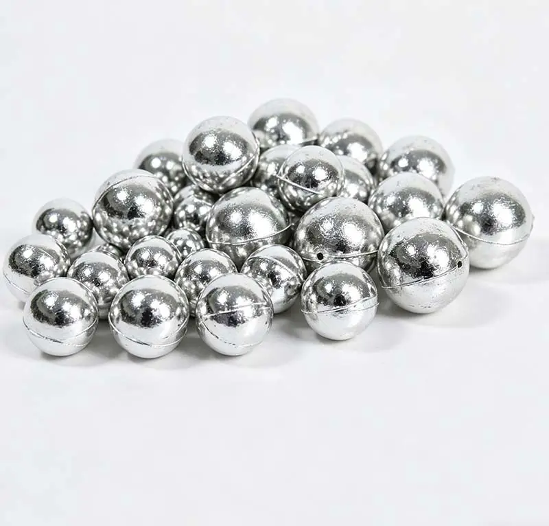
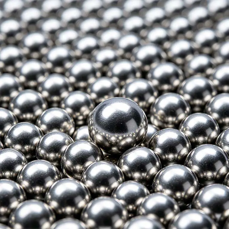
Solder Ball
-
Product Description
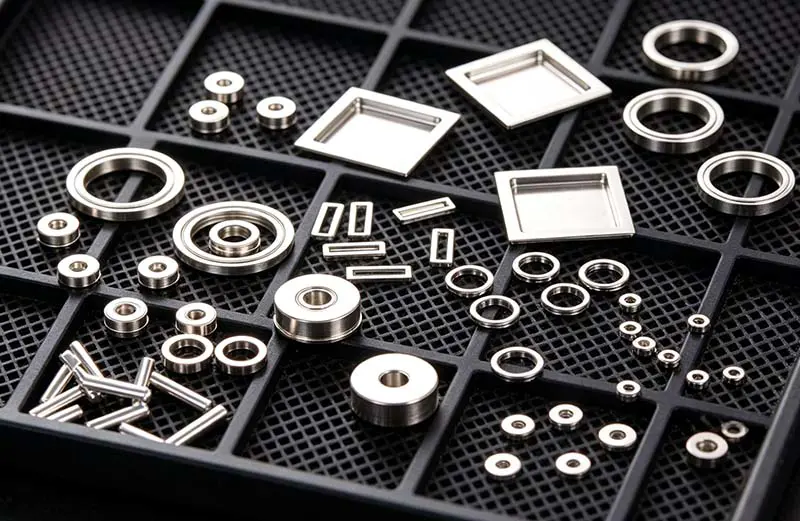
Solder balls are a key interconnect material used in advanced packaging forms such as BGA (Ball Grid Array), CSP (Chip-Scale Packaging) and WLP (Wafer-Level Packaging). By providing stable electrical connections and mechanical support, they enable high-density assembly between the chip package and the printed circuit board (PCB). JFM offers standardized solder ball materials and provides selection guidance to assist customers in choosing the appropriate products based on package type, pitch and assembly process.
Key Features
Solder balls are suitable for high-density electronic packaging applications and possess the following characteristics:
- Good dimensional accuracy and roundness
- Low surface oxidation levels
- Stable mechanical and fatigue resistance properties
- Contributes to improved process consistency
- Suitable for high-reliability packaging scenarios
Application Areas
Solder balls are primarily used in the following packaging and interconnection applications:
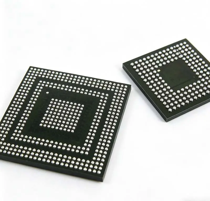
- Semiconductor integrated circuit packaging: Used for interconnections in structures such as BGAs, CSPs and LGAs.
- Wafer-level packaging: Suitable for wafer-level packaging connections requiring very small ball diameters.
- Consumer electronics: Used for the assembly of core processing chips in smartphones, laptops and wearable devices.
- Automotive Electronics: Suitable for high-reliability soldering in in-vehicle computing platforms, sensors and various control modules.
- Communications and networking equipment: Suitable for precision electronic packaging in servers, routers and high-speed communication modules.
Product Specifications
| Parameter Category | Capabilities & Features |
| Processes | brazing and furnace brazing |
| Dimension Capabilities | Suitable for applications requiring tight ball diameter tolerances and good package coplanarity |
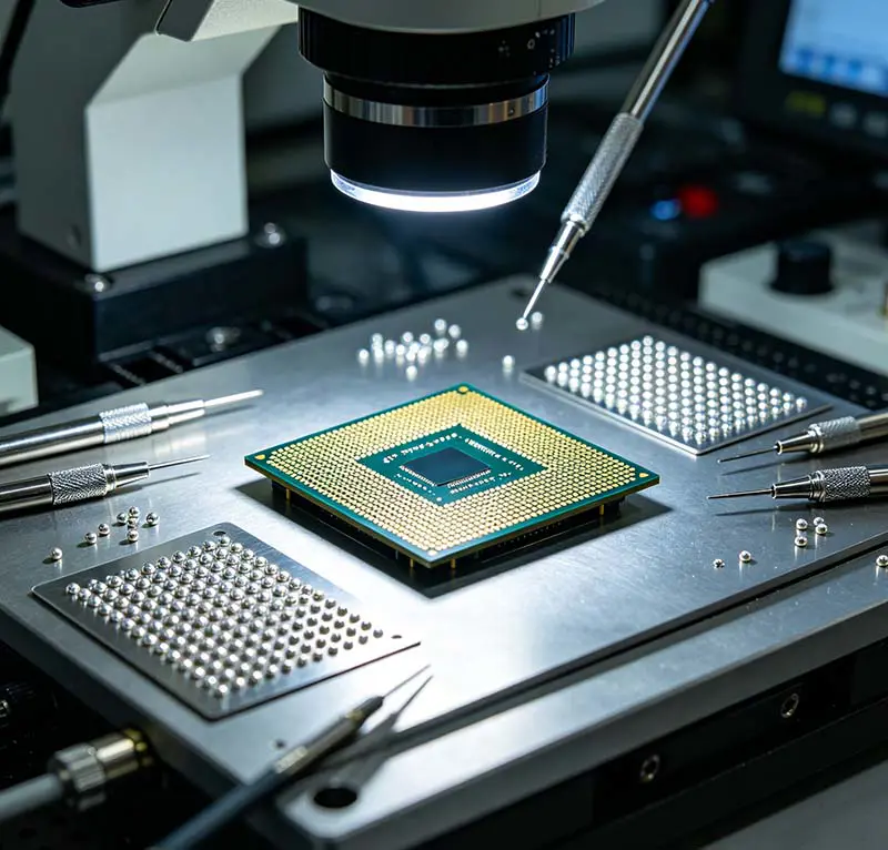
| Compatible Processes | Suitable for processes such as ball placement, wafer/substrate balling, and rework re-balling |
| Applications | Semiconductor bump formation; BGA/CSP interconnections and ball placement; Flip-chip interconnections; Wafer-level balling |
* For further product information and application support, please contact us