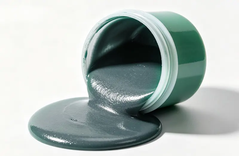
Nano-Silver Paste
-
Product Description
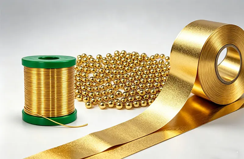
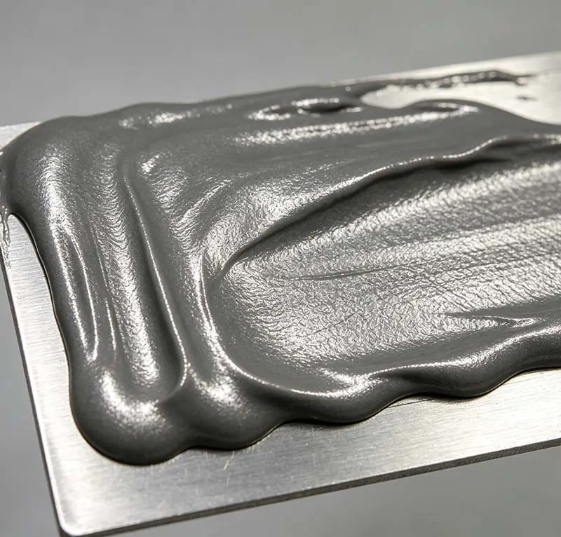
Nano-silver paste is an advanced electronic packaging material that utilizes the surface effects of nanoparticles to achieve low-temperature sintering and high-temperature operation. It offers good thermal and electrical conductivity, optimizing the heat dissipation efficiency and service life of high-power devices. JFM provides high-performance sintering material solutions to meet the stringent application requirements of third-generation semiconductors, high-power LEDs and RF devices for superior thermal management and long-term reliable connections.
Key Features
Designed specifically for high-power-density packaging, nano-silver paste offers the following advantages:
- Good thermal and electrical conductivity
- Low-temperature sintering to form a high-melting-point silver bonding layer
- Good interfacial bonding strength
- Flexible process adaptability
- Helps improve process consistency
- Environmentally friendly and high cleanliness
Application Areas
Nano-silver paste is primarily used in electronic packaging applications where stringent requirements for heat dissipation and reliability apply:
- Third-generation semiconductor packaging: Used for chip bonding in certain power modules to enhance module power density.
- High-power LED packaging: Suitable for bonding heat sinks to heat-sensitive devices such as high-brightness and UV LEDs.
- RF and Microwave Components: Used in high-frequency, high-heat components such as RF power amplifiers in 5G base stations.
- New Energy Vehicle Electronics: Used in core power units such as motor controllers and on-board chargers.
- Photovoltaics and Industrial Power Supplies: Suitable for photovoltaic inverters and industrial power supply modules.
Product Specifications
| Parameter Category | Capabilities & Features |
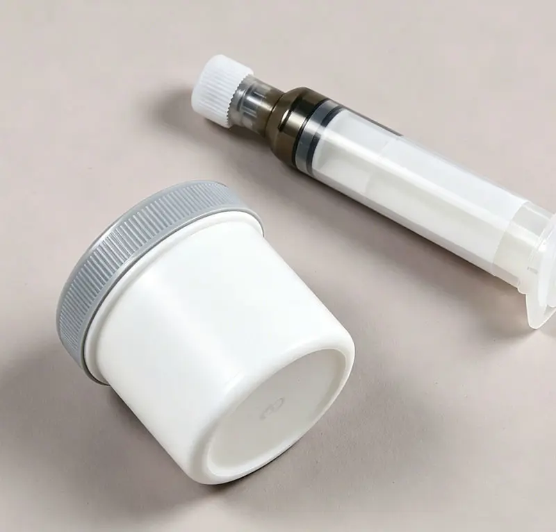
| Product Form | Slurry/paste form; forms a sintered silver layer/body upon heating |
| Sintering Method | Pressure less sintering; tailored solutions provided to meet specific requirements |
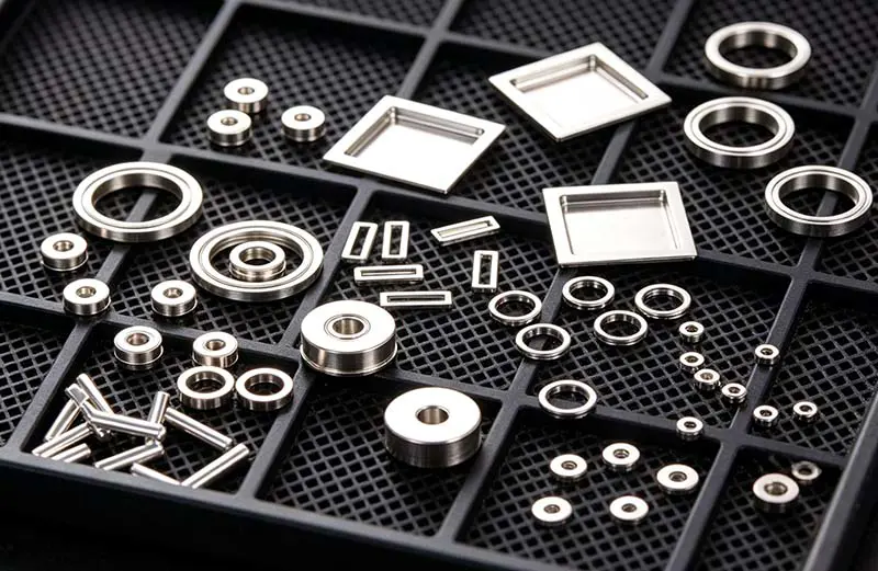
| Applications | Suitable for applications such as power semiconductors and LEDs; specifications can be selected according to different chip sizes and structures |
| Suitable Processes | Supports dispensing, stencil/metal mask printing, and needle transfer methods |
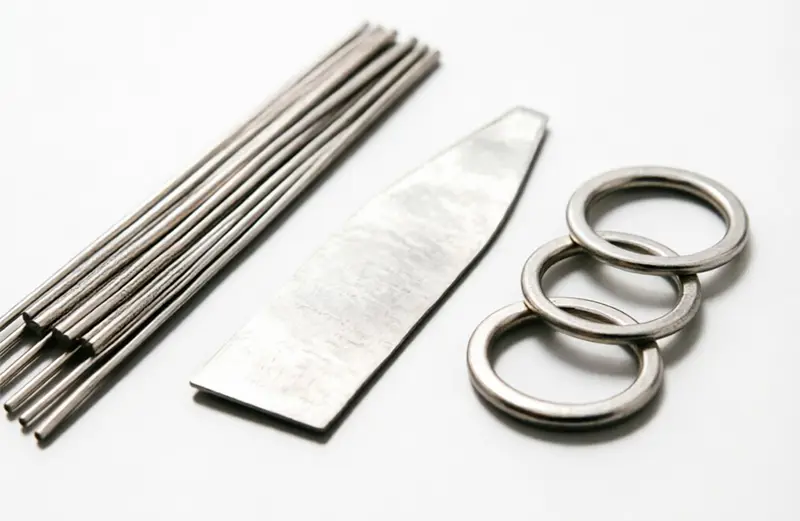
| Suitable Surfaces | Suitable for reliable bonding to a variety of metallized surfaces (e.g. gold-plated, silver-plated, copper, etc.) |
* For further product information and application support, please contact us