Why 99% Alumina Ceramics Are Used in Semiconductor Equipment?
-
2026-08-06 Industry News






Discover why 99% alumina ceramics are widely used in semiconductor equipment, including their high purity, electrical insulation, thermal stability, and reliability.
Introduction
In the field of semiconductor equipment, material selection is never as simple as “the higher the performance, the better”; rather, it is a process of constantly balancing purity, stability, reliability, and cost. For this very reason, 99% alumina ceramics has been used extensively, consistently, and in large quantities in semiconductor equipment for a long time, gradually becoming the “default choice” for many critical non-metallic structural and functional components.
This is neither a coincidence nor a result of market inertia, but rather the outcome of repeated validation through engineering practice.
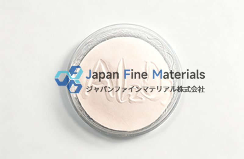
Core Material Requirements for Semiconductors
To understand why 99% alumina ceramics are repeatedly chosen for semiconductor equipment, we must first consider the operating environment and design logic of the equipment itself. Unlike traditional industrial equipment, semiconductor equipment is not primarily characterized by “short cycles and high loads,” but rather emphasizes long-term, stable, and repeatable process performance.
In core equipment such as etching, deposition, diffusion, and cleaning systems, materials are often subjected to a combination of multiple complex operating conditions, such as:
• High-vacuum or ultra-high-vacuum environments, which amplify any potential risk of volatilization or outgassing from the materials
• The combined effects of high-frequency electric fields and plasma place even higher demands on electrical stability and surface durability
• During prolonged continuous operation, gradual changes in material performance are more destructive than instantaneous failures
At the same time, semiconductor processes are extremely sensitive to particulate contamination and metal ions; even trace amounts of release can manifest as yield fluctuations at the statistical level. Therefore, material issues often do not appear as obvious damage but gradually manifest as parameter drift, increased maintenance frequency, or reduced consistency.
Why 99% Grade Aluminum Oxide Instead of Standard Aluminum Oxide?
From an engineering materials perspective, the purity of alumina is not merely a simple classification label, but rather one of the key factorsthat influence the material’s internal microstructure. Differences in purity manifest across multiple levels, including grain morphology, grain boundary composition, and the distribution of impurity phases.
When the purity of alumina is low (e.g., 95% or below), the material typically contains a higher proportion of sintering aids or glass phases. In semiconductor equipment, such materials may gradually reveal the following issues:
• Under high-vacuum or high-temperature conditions, non-alumina components pose a risk of slow volatilization or migration
• In high-frequency electric field environments, electrical insulation performance exhibits more pronounced changes over time or with temperature
• It is more difficult to ensure consistency across different batches of material
In contrast, 99% alumina ceramics have lower impurity levels, typically contain fewer secondary phases and glass phases, and exhibit more predictable grain boundary stability in environments where high temperatures, vacuum, and electric fields are coupled. These advantages are not reflected in any single “standout parameter,” but rather in consistent performance over the long term.
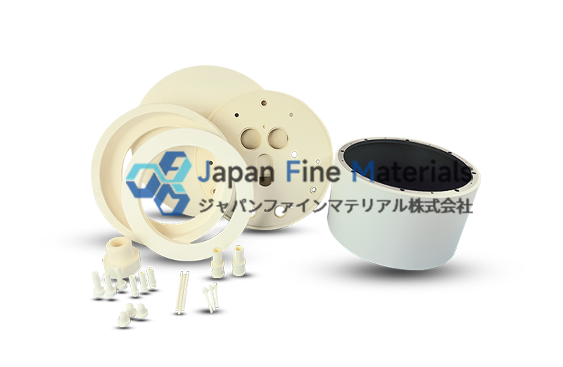
Advantages in Electrical Performance and Plasma Environments
Inside semiconductor equipment, alumina ceramics primarily serve as insulators, barriers, and structural supports. These components are not typically subjected to extreme mechanical loads, but they must meet extremely high requirements for electrical performance consistency and surface stability.
99% alumina ceramics maintain relatively stable dielectric properties under high-frequency electric field conditions and are therefore commonly used as:
• Insulating support structures for electrodes or conductive components
• Isolation components and functional structural parts inside vacuum chambers
• Ceramic components that but do not come into direct contact with wafersareexposed to plasma environments for extended periods
In actual operation, a critical yet often overlooked point is that the electrical properties ofceramics 99% alumina vary with time and temperature generally easier to controland are . This “controllability of variation” is particularly important for the long-term stability of equipment parameters.
Stability is often more important than “peak performance”
A common misconception in material selection is placing excessive emphasis on ultimate performance parameters while overlooking the actual stability requirements of the engineering system. For semiconductor equipment, the more critical consideration is whether the material can maintain predictable and consistent behavior over the long term under specified operating conditions.
Although higher-purity alumina ceramics perform better in certain metrics, this also means:
• a significant increase in cost
• Increased processing difficulty and pressure to maintain yield rates
• Higher demands on supply chain stability
In actual engineering practice, “over-engineering” materials does not necessarily yield corresponding system benefits. For a large number of structural components that do not come into direct contact with wafers but require long-term stable operation, 99% alumina ceramics strike a proven, reasonable balance between performance, manufacturability, and cost.
Engineering Feasibility of 99% Alumina Ceramics
In the semiconductor industry, “mature” does not imply a conservative approach to technology; rather, it signifies that a solution has undergone sufficient engineering validation. In practical applications, the machining processes, quality control methods, and failure characteristics of 99% alumina ceramics are relatively well-defined.
This level of maturity is typically reflected in several aspects:
• Clear forming and sintering process routes
• Mature experience in dimensional control and finishing
• Common failure modes and risk points are well-defined
This enables engineers to assess risks more accurately during the design phase and makes it easier for the manufacturing side to achieve stable delivery. From a systems engineering perspective, this level of maturity can effectively reduce uncertainty and enhance the overall controllability of the project.
Conclusion
The reason 99% alumina ceramics are repeatedly adopted in semiconductor equipment is not because they have the “most impressive specifications,” but because they can operate reliably, stably, and predictably over the long term under real-world operating conditions.
This is precisely the most important—and rarest—quality in the selection of materials for semiconductor equipment.
If you are evaluating or customizing alumina ceramic components for a semiconductor equipment project—whether regarding material purity selection, structural design feasibility, or machining precision—we welcome you to discuss your specific application scenarios with the JFM team.
Based on the principle of suitability for operating conditions: We’ll help you determine 99%whetherare suitable alumina ceramics for your equipment needs—rather than simply recommending materials with “higher specifications”—to provide right for your equipmentthe solution material .
Contact JFM today to bring material selection back to the fundamentals of engineering.