Applications of Semiconductor Ceramics in Modern Chip Manufacturing
-
2026-01-09 Industry News


Advanced ceramic materials play a critical role in semiconductor manufacturing by enabling chip stability and long-term reliability.
Introduce
The semiconductor industry is a critical foundation that supports today’s electronic information society. From smart devices to high-performance computing, electric vehicles (EVs), and 5G communications, chip stability and reliability determine competitiveness across the entire industry. In chip manufacturing, packaging, and testing processes, materials face extremely strict requirements; even slight impurities or variations in material properties can cause yield drops on production lines. High-purity, high-performance ceramic materials—offering excellent electrical insulation, thermal conductivity, plasma-corrosion resistance, and high mechanical strength—have therefore become indispensable key materials in semiconductor manufacturing processes.
What are Semiconductor Ceramics?
Semiconductor ceramics do not refer to "conductive ceramics"; rather, they denote high-performance structural and functional ceramics used in the semiconductor industry. These materials are primarily used in wafer-processing equipment, vacuum chambers, chip packaging, and test jigs.
Compared with conventional ceramics, this class of materials exhibits the following characteristics:
● High purity: effectively prevents contamination from metallic impurities and maintains ultra-clean production environments.
● Excellent electrical insulation: ensures stable electrical system operation under high-voltage and high-frequency conditions.
● Superior thermal conductivity and thermal stability: provide sufficient heat exchange and stable temperature control required by equipment.
● Plasma-corrosion resistance: withstand harsh chemical reactions generated in etching and deposition processes.
● High-precision dimensional and surface quality: meet micron-level tolerances required by modern fine processes.
These properties make ceramics essential components for equipment operation and key materials for chip packaging and testing processes.
Ceramic Parts in Wafer Manufacturing Equipment
1. Vacuum Chuck
Vacuum chucks are critical parts used to hold and transport wafers during semiconductor manufacturing processes and are manufactured from high-performance (fine) ceramics. Their surfaces exhibit high flatness and excellent thermal stability, maintaining stable clamping performance even under high temperature, vacuum, and corrosive conditions—thereby preventing wafer slippage and contamination. Vacuum chucks are used in exposure, etching, and thin-film deposition equipment to ensure wafer positioning accuracy and process consistency.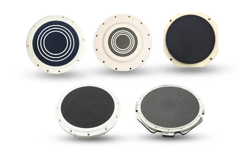
2. Wafer Transfer Arm
Wafer transfer arms are essential elements in automated wafer handling systems, used to transport wafers reliably and efficiently within ultra-clean environments. These parts are made from high-rigidity, corrosion-resistant fine ceramics that offer excellent mechanical strength and wear resistance, enabling stable operation even under high-frequency use. Designs balance light weight and high precision to allow micrometer-level accurate positioning. They are used in wafer-processing equipment, packaging, and testing stages, contributing to improved production-line efficiency and operational stability.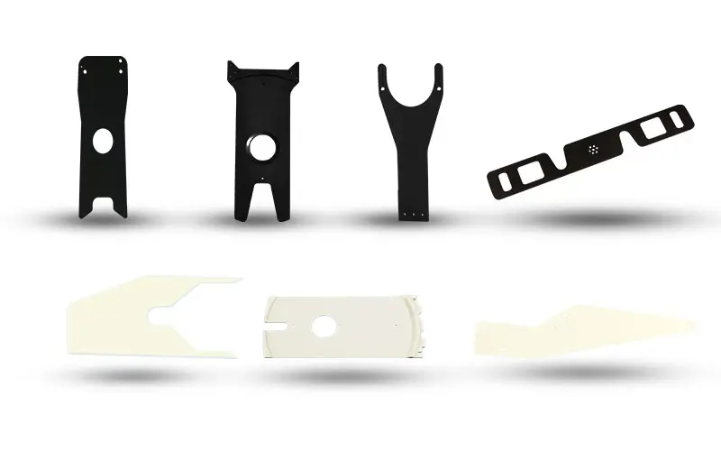
3. Focus Ring and Edge Ring
Focus rings and edge rings are installed around the wafer periphery to tune plasma distribution inside etching chambers and protect wafer edges. Ceramics such as alumina (aluminum oxide) and silicon nitride provide high hardness and corrosion resistance, resisting impacts from high-energy ions and extending ring service life. These rings help optimize etching uniformity, reduce edge-defect rates, improve yield, and decrease maintenance frequency for equipment.
4. Isolation Rings and Insulating Rings
Isolation and insulating rings are placed between electrodes and chamber structural members to provide electrical and thermal insulation. Ceramic materials maintain insulation under high-voltage plasma conditions, preventing arcing and plasma leakage. Their heat resistance ensures stable performance over the long term. Compared with common metals or lower-performance ceramics, these ceramic rings reduce equipment failure rates and maintenance costs while enabling reliable continuous production.
5. Shield Ring
Shield rings are positioned at the chamber edges to protect wafers from the direct impact of high-energy particles and to reduce contamination from sputtered chamber-wall materials. Shield rings made from high-corrosion-resistant or composite ceramics withstand plasma-induced high-energy impacts and extend component life. High-performance ceramic shield rings lower chamber maintenance frequency while ensuring wafer-surface cleanliness and production-line stability.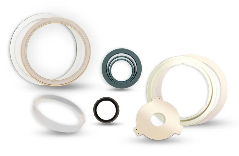
Ceramic Parts for Chip Packaging and Testing Processes
1. Ceramic Substrates (HTCC / LTCC)
Ceramic substrates are critical support materials in power semiconductors, RF chips, and high-performance IC packaging. High-purity alumina, aluminum nitride, and silicon nitride ceramics provide low dielectric constant, superior thermal conductivity, and dimensional stability—significantly improving signal transmission and heat dissipation for chips. This reduces thermal stress in power devices and enhances device reliability. Additionally, they ensure connection stability in high-density packaging, meeting the high-performance and high-reliability requirements of industrial chip packaging.
2. Ceramic Packages
Ceramic packages are used for high-frequency, RF, and power chips. Their high-temperature resistance, low dielectric loss, and excellent hermeticity protect chips from environmental moisture and chemical corrosion, ensuring long-term reliability. Compared with plastic packages, ceramic packages excel in high-reliability applications such as automotive electronics and critical semiconductor components, reducing device failure rates.
3. Ceramic Probe Cards & Test Sockets
In wafer testing, ceramic probe cards and test sockets provide high-rigidity support and electrical insulation, maintaining high-precision positioning and test pin repeatability. The low coefficient of thermal expansion of ceramics ensures stability during high-density testing and extended operation, reducing test errors, lowering repair rates, and improving production efficiency.
Semiconductor Industry Common Ceramic Materials
Alumina (Al₂O₃)
Alumina (Al₂O₃) is a fundamental ceramic material with high insulation, chemical stability, and excellent mechanical strength. It is widely used in critical parts such as vacuum chucks, transfer arms, isolation rings, and focus rings. High-purity alumina effectively blocks high-voltage current and endures long-term continuous operation in plasma environments.
Zirconia (ZrO₂)
Zirconia (ZrO₂) offers excellent toughness and wear resistance, withstanding stresses in complex structural parts subject to mechanical friction and impact. It is used in edge rings, shield rings, and other wear-prone components, contributing to extended part lifetimes and stabilized process continuity and yield.
Aluminum Nitride (AlN)
Aluminum nitride (AlN) features excellent thermal conductivity and a low coefficient of thermal expansion, playing a key role in ceramic heaters and thermal-management substrates. By evenly and stably transmitting heat, AlN maintains wafer temperature stability during deposition and etching, reducing thermal stress and thin-film thickness variation. AlN ceramics are particularly important in power devices and high-performance IC packaging where thermal treatment and high-frequency performance are required.
Silicon Nitride (Si₃N₄)
Silicon nitride (Si₃N₄) exhibits high thermal-shock resistance and mechanical strength, and is widely used for focus rings, edge rings, and various load-bearing structural components. It is indispensable in high-stress, high-corrosion process environments—maintaining dimensional accuracy and structural stability under prolonged high temperatures and plasma exposure within etching equipment chambers.
Silicon Carbide (SiC)
Silicon carbide (SiC) ceramics combine excellent thermal conductivity, high hardness, chemical stability, and a coefficient of thermal expansion similar to silicon. They are used in wafer manufacturing and chip packaging processes as base materials for vacuum chucks, heater disks, and ceramic rings. Under complex operating conditions such as high power and high frequency, SiC maintains stable mechanical performance and electrical insulation, optimizing equipment durability and process consistency to support high-yield chip manufacturing.
Porous Ceramics
Porous ceramics are primarily made from high-quality raw materials such as alumina, silicon carbide, and cordierite and are produced through forming and specialized high-temperature firing processes. We provide porous ceramic products with customizable pore sizes and porosity according to customer needs. These products feature high flatness and parallelism, uniform and dense microstructures, and are easy to machine and modify. They are widely used in wafer inspection, dicing, and screen printing processes and are essential components in grinders, dicing equipment, and cleaning equipment for processing wafers and large panels of various sizes.
Conclusion
Ceramics play a vital role in the semiconductor industry. In wafer manufacturing, they ensure process stability and chamber cleanliness; in packaging and testing, they provide reliable insulation, heat dissipation, and structural support. In other words, ceramics are not merely important components but foundational materials that support the reliability of chip fabrication and application.
If you are considering high-performance semiconductor ceramic solutions, please contact JFM. We focus on manufacturing and customizing a wide variety of ceramic parts and provide solid technical expertise and reliable support.


