Applications of Silicon Carbide Ceramics in Semiconductors
-
2026-05-18 Industry News


Learn about silicon carbide semiconductor applications in power electronics, RF devices, and high-frequency systems, including efficiency, thermal stability, and high-voltage performance.
Introduction
Semiconductor manufacturing processes are continuously evolving toward higher precision, higher power, and higher temperatures. Consequently, equipment materials are subject to increasingly stringent requirements, particularly in critical stages such as wafer handling, epitaxial growth, etching, ion implantation, and optical inspection. Thanks to its high-temperature resistance, chemical stability, high mechanical strength, and excellent dimensional stability, silicon carbide (SiC) ceramic has gradually emerged as a vital material in semiconductor equipment.
The advantages of silicon carbide ceramics are not limited to individual components; rather, their application across different process stages synergistically enhances the overall performance of the equipment. As the semiconductor industry continues to evolve, the potential of silicon carbide in future high-precision microstructures, power modules, and innovative process designs is becoming increasingly evident.
Core Properties of Silicon Carbide Ceramics
The value of silicon carbide ceramics in semiconductor equipment stems from their unique material properties:
• High-Temperature Resistance: Helps maintain dimensional and shape stability in high-temperature process environments, reducing process variations.
• Chemical Stability: Exhibits excellent resistance to fluorinated gases, chlorinated gases, and other highly reactive chemicals, making it suitable for etching equipment and ion implantation environments.
• High mechanical strength and wear resistance: Delays component wear during wafer handling, rotary support, or high-load environments, enhancing equipment operational stability.
• Low thermal expansion coefficient: Minimizes micro-deformation in high-temperature environments, contributing to the repeatability and stability of precision processes.
• Good thermal conductivity: Aids in thermal management within high-power devices and modules, reducing temperature gradients.
These properties make silicon carbide ceramics one of the preferred materials for semiconductor manufacturing equipment design and process optimization. Particularly in high-precision processes such as wafer handling and epitaxial growth, material stability directly impacts product quality and production efficiency.
Applications in Wafer Handling
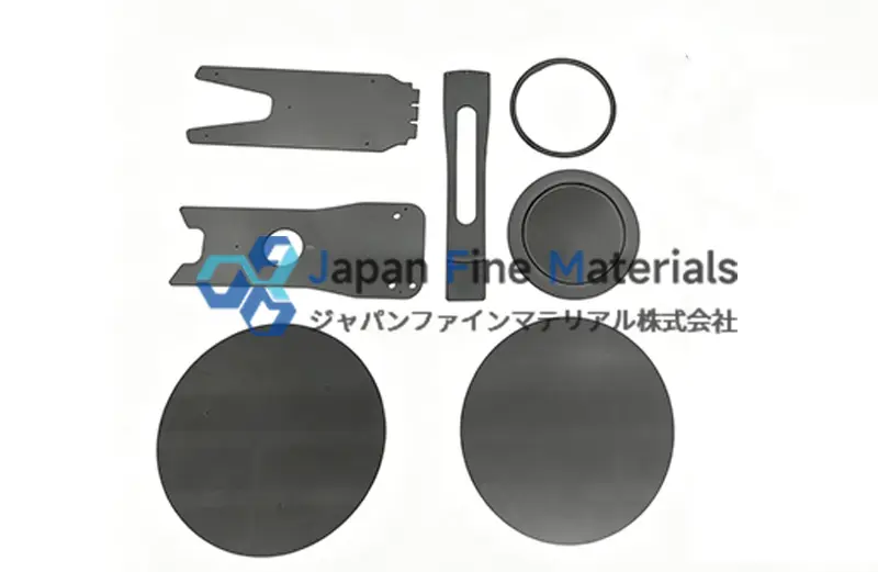
Silicon Carbide Arms and Handling Precision
Wafer handling is a fundamental and critical step in semiconductor manufacturing; its precision directly impacts wafer yield and the effectiveness of subsequent processes. Silicon carbide ceramic arms play a central role in the handling process, not only providing stable support but also minimizing minor deviations caused by thermal expansion and vibration.
Silicon carbide arms maintain path accuracy under high-temperature or continuous operation conditions. Their low thermal expansion and high rigidity ensure that minor temperature fluctuations do not cause wafer displacement, thereby reducing the risk of breakage. This is particularly important for large-size wafers or multi-layer processes, as even the slightest deviation can affect lithography or etching accuracy.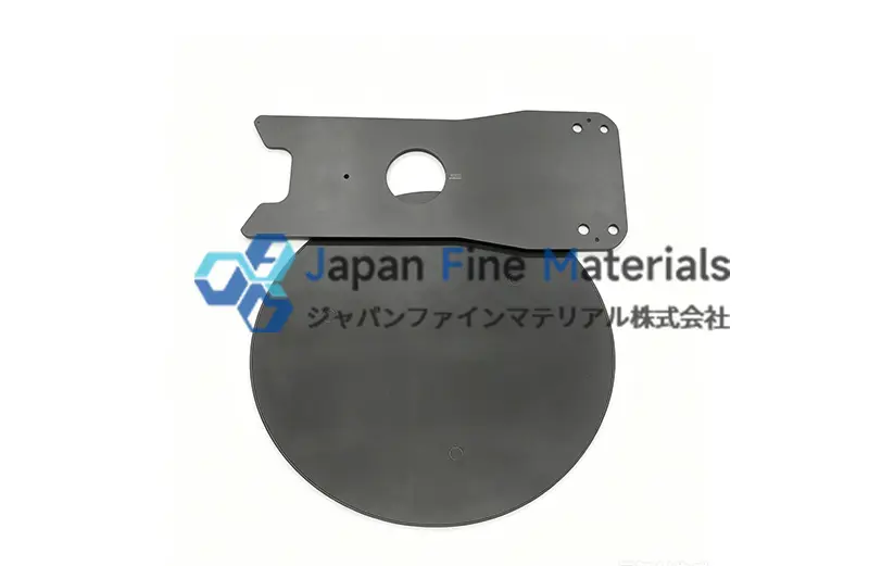
Optimized Carrier Trays and Pad Suction Cups
Bumper pads and carrier trays optimize the pressure distribution at wafer contact points, helping to reduce friction and minimize the likelihood of micro-scratches. To further enhance handling stability, the design of silicon carbide arms and suction pads can incorporate computational fluid dynamics (CFD) and finite element analysis (FEA) for microstructural adjustments, thereby mitigating the effects of vibration, shock, and thermal deformation.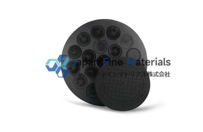
Additionally, surface microstructures or nano-coating technologies can improve adhesion and friction characteristics while helping to extend component lifespan.
• Improving Handling Precision and Reducing Deviation
• Reducing friction and wafer surface damage
• Improving handling stability and repeatability
Adaptability to large-size wafers and complex multi-layer processes
Epitaxial growth and rotary support components
The Role of Epitaxial Rings in Wafer Positioning
The epitaxial ring plays a central supporting role in the wafer epitaxial growth process, primarily used to maintain stable wafer positioning in high-temperature environments. Its low thermal expansion properties help minimize micro-displacements caused by thermal stress, thereby improving wafer thickness uniformity and surface flatness. In high-temperature or long-duration operating environments, the stability of the epitaxial ring directly impacts epitaxial growth consistency and yield.
By optimizing the microstructure of the epitaxial ring, the impact of temperature fluctuations on wafer positioning can be further reduced, helping to improve the precision and repeatability of the epitaxial process.
Optimization of Bearing Sleeve and Thermal Management Design
Shaft sleeves bear loads in rotating equipment, helping the equipment maintain mechanical precision and structural stability during high-speed or prolonged operation. In terms of design optimization, the high mechanical strength and thermal conductivity of silicon carbide ceramics can be leveraged by incorporating micro-heat dissipation grooves or highly thermally conductive composite materials into the shaft sleeves and epitaxial rings. This not only improves heat distribution but also reduces the risk of localized wafer overheating, further enhancing the consistency and stability of epitaxial growth.
By simulating heat flux and mechanical loads, component geometries can be optimized to achieve design solutions that balance lightweight construction with high rigidity.
• Optimizing the microstructure of the epitaxial ring to improve wafer thickness uniformity
• Selection of bushing materials and thermal management design to improve equipment operational stability
Integration of composite materials or heat dissipation grooves to optimize heat distribution in high-temperature environments
The Role of Silicon Carbide Baffles in Etching Equipment
Etching is a technically challenging process in semiconductor manufacturing, imposing stringent requirements on equipment materials regarding high-temperature resistance, chemical stability, and mechanical strength. Gas flow within the reaction chamber significantly influences etching uniformity, and silicon carbide baffles play a central role in this process. Through precise geometric design, the baffles guide gas to distribute uniformly across the wafer surface, reducing the risk of localized over-etching and etching defects, thereby improving process consistency.
The chemical stability of silicon carbide allows the baffle to withstand long-term use in environments containing fluorinated and chlorinated gases, reducing the likelihood of chemical corrosion and particulate contamination. At the same time, its high mechanical strength and wear resistance ensure the long-term operational reliability of the equipment. In practical applications, optimizing the microstructure of the baffle can improve gas flow paths, enhance etching precision, and reduce the accumulation of localized thermal loads.
• Improved gas flow distribution enhances etch uniformity
• Reducing the risk of localized over-etching and etching defects
• Enhancing the equipment’s corrosion and wear resistance
• Supporting long-term operation in high-temperature and chemically active environments
Through these design and material optimizations, silicon carbide baffles not only meet the requirements of existing etching processes but also provide a stable material foundation and process feasibility for future high-precision microstructure etching.
Flow Plate Optimization in Ion Implantation Equipment
During the ion implantation process, flow plates and internal components of the target chamber are subjected to high-energy ion bombardment and localized high-temperature environments. The wear resistance and mechanical strength of silicon carbide flow plates provide reliable support while indirectly regulating ion beam distribution, thereby reducing the likelihood of wafer dose non-uniformity.
Through surface microstructure optimization or composite coating designs, the stability of the ion beam path can be further improved, enhancing implantation accuracy while delaying equipment wear and reducing maintenance frequency.
• Improving Etching Uniformity and Consistency
• Optimizing Ion Beam Path Distribution
• Delaying equipment wear and reducing maintenance frequency
Supports long-term use in high-temperature and chemically active environments
The Role of Silicon Carbide Grating Plates in Optical Inspection
Silicon carbide grating plates play a central role in photolithography and optical inspection processes. These components must maintain precise shapes and dimensions under high-temperature and high-intensity light conditions, while ensuring that performance is not compromised by chemical gases or particulate contamination during long-term use. The low thermal expansion properties of silicon carbide ceramics allow the grating plates to maintain flatness in environments with temperature fluctuations, thereby reducing optical inspection errors and enhancing the reliability of precision measurements and microstructure alignment.
Furthermore, the high mechanical strength and wear resistance of silicon carbide grating plates ensure stable performance during prolonged and repeated use, reducing the frequency of replacement and maintenance. Combined with precision microstructure machining and surface coating treatments, the reflective and refractive properties of the grating plates can be further optimized, thereby enhancing the overall performance of optical inspection equipment.
• Maintains dimensional and shape stability in high-temperature environments
• Resistance to chemical gases and particulate contamination
• Improved measurement accuracy and optical positioning reliability
• Supports long-term repeated use, reducing maintenance costs
Through these optimizations, silicon carbide grating plates not only improve the accuracy of existing optical inspection but also provide a stable material foundation for future nanoscale lithography and high-precision microstructure inspection.
Optimization of Microstructure Support Components
Microstructure support components provide stable support beneath critical optical elements, reducing misalignment caused by vibration or thermal stress. Particularly in nanoscale lithography or ultra-high-precision inspection, even minor deviations can directly impact device yield; therefore, the dimensional stability and wear resistance provided by silicon carbide ceramics are critical requirements.
• Maintaining Dimensional and Geometric Stability at High Temperatures
• Reduction of displacement caused by vibration or thermal stress
• Extend equipment cleaning cycles and reduce maintenance costs
• Providing reliable support for nanoscale lithography and high-precision measurement
Silicon carbide microstructure support components not only meet current optical inspection requirements but also provide material assurance and design possibilities for future high-precision, nanoscale packaging and complex microstructure equipment.
Conclusion
As demonstrated by wafer handling, epitaxial growth, etching, ion implantation, and optical inspection and analysis, silicon carbide ceramics not only offer individual performance advantages but also enhance overall equipment performance through synergy across different process steps. By combining material selection, geometric optimization, and thermodynamic and fluid dynamics simulations, their full potential can be realized, contributing to improved wafer yield and process stability.
With the increasing size of wafers and the widespread adoption of 3D packaging and high-power devices, there remains significant room for expansion in the application of silicon carbide ceramics in microstructure support, thermal management, and adaptation to new processes.
For information on customized application solutions, process optimization designs, and future potential applications of silicon carbide ceramics in semiconductor manufacturing equipment, please contact JFM for professional consultation and support.


