What Is an Electrostatic Chuck? A Complete Guide
-
2026-09-09 Industry News






Learn what an electrostatic chuck is, how it works, its main types and materials, and how ESCs are used for wafer handling and semiconductor processing.
Introduction
In the semiconductor manufacturing process, wafers must maintain precise positioning during processes such as etching, thin-film deposition, and ion implantation, while also withstanding varying temperatures, electric fields, and vacuum environments. Traditional mechanical clamping methods may exert contact pressure on the wafer surface; therefore, the electrostatic chuck has gradually become a critical component in wafer processing equipment.
An electrostatic chuck uses electrostatic forces to attract and secure the wafer, eliminating the need for direct clamping via mechanical fixtures. In addition to providing wafer clamping functionality, its structural design is closely related to process factors such as wafer temperature control, back-side gas control, and particle management.
So, what exactly is an electrostatic chuck? How does it work? And why do semiconductor equipment manufacturers use this type of chuck?
What Is an Electrostatic Chuck?
An electrostatic chuck is a holding device that uses electrostatic forces to secure wafers or other thin substrates; it is primarily used in semiconductor manufacturing and related precision processing equipment.
Unlike vacuum chucks, which rely on vacuum pressure to secure workpieces, electrostatic chucks typically feature electrodes embedded within a ceramic substrate. When a direct current (DC) voltage is applied to the electrodes, an electric field forms on the chuck’s surface, generating an electrostatic force between the wafer and the chuck, thereby helping to hold the wafer in place.
Depending on the electrode structure and operating mode, electrostatic chucks can be designed in various ways, such as:
• Unipolar Electrostatic Chuck
• Bipolar electrostatic chucks
• Multi-zone electrode structure
• Electrostatic chucks with heating elements
• Electrostatic chucks with rear gas channels
Therefore, an electrostatic chuck is not simply a ceramic plate that holds a wafer in place, but rather a precision component involving ceramic materials, electrode design, surface finishing, temperature control, and gas channel design.
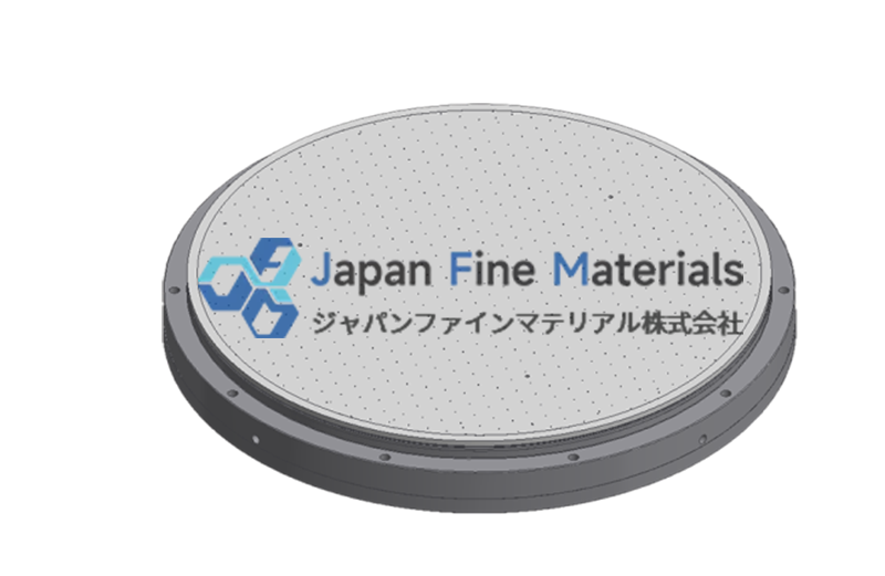
Main Structure of an Electrostatic Chuck
An electrostatic chuck used in semiconductor equipment typically consists of multiple functional structures.
Ceramic Substrate
The ceramic substrate is a critical component of the electrostatic chuck, primarily serving as an insulator, a support structure, and a dielectric.
Common materials include:
• Aluminum oxide
• Aluminum nitride
• Other ceramic materials suitable for specific process conditions
Different ceramic materials vary in terms of thermal conductivity, electrical resistivity, dielectric properties, and thermal expansion characteristics; therefore, the choice must be made based on the specific process.
Internal Electrodes
The electrodes are responsible for generating the electrostatic field; their shape, thickness, position, and the distance between them all affect the electric field distribution.
Electrode structures may be designed differently for different wafer sizes and processing equipment. Multi-zone electrodes also allow for region-specific control to accommodate more complex process requirements.
Adhesion Surface
The gripping surface is in direct contact with the wafer; therefore, its flatness, roughness, microstructure, and particle condition all affect the contact between the wafer and the electrostatic chuck.
Some electrostatic chucks are designed with microscopic protrusions or specific contact structures on their surfaces, which reduce the overall contact area between the wafer and the chuck while providing space for gas flow beneath the wafer.
Gas Channels
In some semiconductor processes, back-side gases such as helium are introduced through gas channels on the back of the electrostatic chuck.
Back-side gas is typically used to improve heat exchange between the wafer and the chuck, thereby aiding in wafer temperature control. Therefore, the layout, dimensions, and sealing area design of the gas channels are also critical components of the electrostatic chuck’s structure.
Heating Structure
Some electrostatic chucks incorporate heating functionality to regulate wafer temperature via heaters.
In processes such as plasma etching, wafer temperature affects material removal rates, reaction processes, and process consistency; therefore, the thermal management design of the electrostatic chuck holds significant process value.
How Does an Electrostatic Chuck Work?
The basic operating process of an electrostatic chuck can be understood in three stages: applying voltage, generating electrostatic adhesion, and releasing the wafer.
1. Applying Voltage
The interior of an electrostatic chuck typically contains a layer of conductive electrodes. When the equipment applies a DC voltage to the electrodes, an electric field forms around them.
If the electrostatic chuck employs a bipolar structure, positive and negative electrodes are usually distributed in different areas within the chuck, thereby creating a corresponding electric field distribution.
2. Generating Electrostatic Adhesion
Once the wafer is placed on the surface of the electrostatic chuck, the electric field generates an electrostatic attractive force between the wafer and the electrodes inside the chuck. For conductive wafers (such as silicon wafers), a charge opposite to that of the electrodes is induced on their surface; for insulating wafers, the force is generated through dielectric polarization. This force causes the wafer to adhere tightly to the surface of the chuck.
Unlike mechanical clamping, this method does not require the wafer to be clamped directly at the edges by the chuck, making it well-suited for meeting the spatial and surface requirements of certain precision wafer processing applications.
Electrostatic adhesion depends on several factors, including:
• Applied voltage
• Electrode structure
• Ceramic dielectric properties
• The gap between the wafer and the suction cup
• Contact conditions
• Surface roughness
• Material Resistivity
Therefore, the adhesion performance of an electrostatic chuck cannot be determined by a single parameter alone; it must be analyzed in conjunction with the specific structure and process conditions.
3. Releasing the Wafer
Once wafer processing is complete, the voltage must be reduced or turned off to allow the electrostatic holding force to gradually weaken.
Some electrostatic chucks also require a de-adhesion process to facilitate the separation of the wafer from the chuck surface. If residual charge is not properly managed, it may affect the wafer handling process; therefore, the de-adhesion design is also a critical component of the electrostatic chuck.
Common Ceramic Materials for Electrostatic Chucks
Material is one of the key factors to consider when selecting an electrostatic chuck.
Alumina Ceramics
Alumina possesses good electrical insulation properties, heat resistance, and chemical stability, and is therefore widely used in ceramic electrostatic chucks.
Alumina of different purities and formulations exhibits variations in resistivity, dielectric properties, and mechanical properties. Therefore, in practical design, one cannot rely solely on the material name “alumina”; evaluation must also take into account specific grades and process parameters.
Aluminum Nitride Ceramics
Aluminum nitride has high thermal conductivity and good electrical insulation properties, making it suitable for certain semiconductor processing scenarios with stringent thermal management requirements.
For example, in equipment requiring wafer temperature control, the thermal conductivity of aluminum nitride provides an excellent material foundation for heat transfer.
Why Are Ceramics Suitable for Electrostatic Chucks?
Due to their high resistivity, high dielectric strength, excellent thermal stability, and chemical inertness, ceramic materials are an ideal choice for manufacturing the substrate of electrostatic chucks (ESCs). These properties enable them to withstand the high-voltage electric fields, plasma etching, and severe thermal cycling shocks encountered during ESC operation, whereas metal or polymer materials are prone to failure under such harsh conditions.
However, material requirements vary depending on the specific process. For example, if the equipment prioritizes heat dissipation performance, aluminum nitride should be evaluated as a primary option; if the focus is on material cost, insulation performance, and process compatibility, a comprehensive comparison should be made that includes materials such as aluminum oxide.
Main Applications of Electrostatic Chucks
Electrostatic chucks are primarily used in equipment related to semiconductor and precision electronics manufacturing.
Wafer Etching
During plasma etching, the wafer must be held in a specific position while also undergoing temperature control.
Electrostatic chucks secure wafers using electrostatic forces and, in conjunction with back-side gas flow and temperature control systems, provide the necessary wafer clamping and thermal management conditions for the etching process.
Thin-Film Deposition
In PVD, CVD, and certain other thin-film deposition processes, wafers must be maintained in a specific position and orientation.
An electrostatic chuck serves as a wafer-holding and clamping component and integrates temperature control functions according to the equipment design.
Ion Implantation
During the ion implantation process, wafers must be positioned according to process requirements. Electrostatic chucks can be used to secure wafers and, depending on the equipment design, participate in related thermal management processes.
Semiconductor Testing Equipment
Some wafer inspection and measurement equipment also utilizes precision substrate clamping structures. For applications requiring reduced mechanical contact or stable wafer positioning, the electrostatic chuck can be a viable option.
Advantages of Electrostatic Chucks
Compared to traditional mechanical clamping methods, the key features of electrostatic chucks stem from their electrostatic clamping principle.
Reduced Mechanical Contact
Electrostatic chucks primarily secure wafers through electrostatic forces, eliminating the need to apply clamping force from the edges using traditional mechanical fixtures.
This is particularly significant in process environments where wafer surface space is limited and the edge areas need to remain unobstructed.
Suitable for Vacuum Processes
Many processes in semiconductor manufacturing are carried out in a vacuum environment. Since electrostatic adhesion does not rely on the negative pressure seal of traditional vacuum chucks as its primary clamping mechanism, it can be used in certain vacuum process equipment.
Facilitates Wafer Temperature Management
Some electrostatic chucks can integrate heating structures and rear gas channels, enabling thermal management of the wafer through the coordination of different structural elements.
Enables Regionalized Control
Depending on the equipment design, electrostatic chucks can incorporate multi-zone electrode structures to enable independent control of different zones, providing design flexibility for localized process management during wafer processing.
Electrostatic Chucks vs. Vacuum Chucks
Both electrostatic chucks and vacuum chucks can be used to secure wafers, but their operating principles differ significantly.
|
Comparison Points |
Electrostatic Chuck |
Vacuum Suction Cup |
|
Principle of Operation |
Electrostatic adhesion |
Vacuum Pressure Adhesion |
|
Primary Driving Force |
Electric Field |
Pressure Differential |
|
Wafer Contact Method |
Electrostatic Clamping |
Vacuum Suction |
|
Vacuum Environment Compatibility |
Suitable for certain vacuum processes |
Depends on the specific vacuum configuration |
|
Temperature Control |
Heating and back-side gas systems can be integrated |
Depends on the design |
|
Common Applications |
Semiconductor etching, deposition, etc. |
Wafer handling, inspection, processing, etc. |
It is important to note that there is no simple “one is better than the other” relationship between the two. The actual choice must be determined by considering the process environment, wafer size, temperature requirements, vacuum conditions, clamping method, and equipment configuration.
How to Choose the Right Electrostatic Chuck?
For semiconductor equipment manufacturers and wafer processing companies, the following aspects should be prioritized when selecting an electrostatic chuck.
1. Wafer Size
Different equipment corresponds to different wafer specifications; for example, 200 mm and 300 mm wafers differ in chuck size, electrode layout, and surface structure.
Therefore, the basic dimensions of the electrostatic chuck must first be determined based on the equipment specifications.
2. Ceramic Material
Select the appropriate ceramic material based on process temperature, thermal management requirements, electrical performance, and the chemical environment.
Aluminum oxide and aluminum nitride are common choices, but the specific material must still be evaluated based on actual process conditions.
3. Electrode Structure
The electrode design affects the electrostatic field distribution and clamping performance. For applications requiring localized control, a multi-zone electrode design should also be considered.
4. Temperature Control Methods
If the electrostatic chuck is used for plasma etching or other processes that are sensitive to wafer temperature, attention must be paid to the heating structure, heat conduction paths, and the design of the back-side gas channels.
5. Surface Precision
Since the electrostatic chuck comes into direct contact with the wafer, attention must be paid to flatness, surface roughness, microstructure, and particle control.
6. Customization Capabilities
Different semiconductor equipment may have varying requirements regarding the dimensions, electrodes, gas channels, heating zones, and mounting methods of the electrostatic chuck.
For non-standard equipment, in addition to the product’s specifications, it is important to verify whether the manufacturer possesses the design and fabrication capabilities to customize electrostatic chucks.
Conclusion
An electrostatic chuck is a functional component designed for clamping wafers and precision substrates; its core principle involves generating an adhesive force through electrostatic forces. Compared to conventional mechanical clamping and vacuum suction methods, electrostatic chucks feature distinct design characteristics in areas such as wafer positioning, compatibility with vacuum processes, and temperature management.
From ceramic materials and electrode structures to rear gas channels, heating structures, and surface precision, every aspect influences the final product design. Therefore, when selecting an electrostatic chuck, a comprehensive evaluation should be conducted based on specific equipment and process conditions, rather than comparing a single parameter in isolation.
JFM specializes in the research, development, and manufacturing of ceramic components for semiconductor and precision machining applications. Based on your equipment requirements, wafer size, ceramic material, electrode structure, and thermal management needs, JFM can work with you to explore electrostatic chuck solutions tailored to your project.
If you are evaluating a new electrostatic chuck or seeking a custom ceramic chuck, please contact JFM, and we will discuss your requirements and application conditions with you.